Your board has 47 ECOs (Engineering Change Orders). Assembly yield dropped to 68%. The BOM cost exceeds competitors by 40%. Three critical components are obsolete with no replacements. Sound familiar?
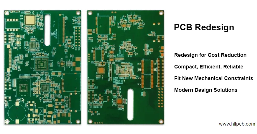
Sometimes, incremental fixes create more problems than they solve. Complete PCB redesign—though initially costly—often delivers dramatic improvements impossible through modification alone.
Real Example: Network switch manufacturer struggled with $127 BOM cost, 73% assembly yield, thermal shutdown issues. After redesign: $52 BOM cost (59% reduction), 94% assembly yield, 15°C cooler operation, 40% smaller footprint. ROI achieved in 4 months.
The Redesign Decision Matrix: Quantifying When to Start Over
Determining whether to modify or completely redesign a PCB requires both technical and financial evaluation. The Redesign Decision Matrix provides an objective framework by assigning points to key technical debt indicators such as excessive ECOs, low assembly yield, high BOM cost, obsolete components, thermal or EMC issues, and power or size constraints. A total score of 0–2 suggests minor modifications are sufficient, 3–4 points indicate the need for a targeted upgrade, 5–6 points justify a full redesign, and 7–8 points signal that redesign is critical to product performance and manufacturability.
To complement this technical analysis, a financial ROI formula can further justify the decision: Redesign ROI = [(Annual Savings × Product Lifetime) - Redesign Cost] ÷ Redesign Cost × 100%. If the ROI exceeds 200%, the redesign is not only technically necessary but also financially advantageous, ensuring long-term efficiency, reliability, and cost-effectiveness.
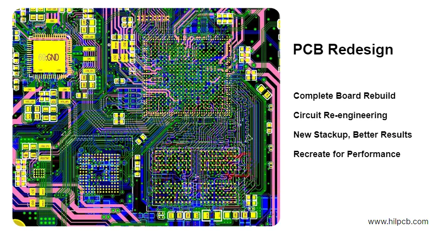
PCB Redesign Architecture: Building from First Principles
System Architecture Reimagining
Traditional Approach (Problematic):
- Start with existing schematic
- Make incremental improvements
- Preserve legacy decisions
- Result: 15-20% improvement
First Principles Redesign (Our Method):
- Define core functionality requirements
- Select optimal modern architecture
- Choose best-in-class components
- Result: 50-80% improvement
Case Study: Industrial Motor Controller Redesign
Original 2012 Design:
- 8-layer board, 200mm × 150mm
- Discrete gate drivers + MCU + separate power stage
- $89 BOM, 127 components
- 12W power dissipation
2025 Redesigned Architecture:
- 4-layer board, 120mm × 80mm
- Integrated smart power module with built-in protection
- $34 BOM, 43 components
- 3.8W power dissipation
- Added: CANbus, predictive maintenance, cloud connectivity
HDI Technology for Miniaturization
Standard PCB → HDI Redesign Results:
- Layer reduction: 8 layers → 6 layers (via-in-pad allows component placement over vias)
- Size reduction: 40-60% smaller footprint
- Cost impact: +$8-12 per board, but saves $20-30 in components and assembly
- Signal integrity: 50% shorter traces improve timing margins
Real measurements from customer redesigns:
- Smartphone accessory: 42mm × 28mm → 24mm × 16mm
- IoT gateway: 100mm × 100mm → 65mm × 65mm
- Wearable device: 35mm diameter → 22mm diameter
Component Selection Strategy in Modern PCB Redesign
The 80/20 Component Rule
In most PCB redesigns, 20% of components drive 80% of cost and complexity. Focus redesign efforts here:
High-Impact Components to Optimize:
- Processors/MCUs: Modern options offer 10x performance at 50% cost
- Power Management: Integrated PMICs replace 10-20 discrete regulators
- Connectors: Modern high-density options save 60% board space
- Passive Arrays: Replace dozens of discrete resistors/capacitors
- Analog Front-Ends: Integrated AFEs eliminate complex discrete designs
Strategic Component Consolidation
Before Redesign: Wireless sensor node
- Nordic nRF52832 (BLE only)
- External 2.4GHz PA
- Separate sub-GHz radio
- External flash memory
- Power management (5 regulators)
- Total: 89 components, $31.20
After Redesign: Same functionality
- Nordic nRF52840 (BLE + Thread + Zigbee)
- Integrated PA in module
- Built-in multi-protocol radio
- Internal 1MB flash
- Single PMIC
- Total: 34 components, $14.80
Thermal Redesign: Eliminating Cooling Hardware
Proper thermal redesign often eliminates fans, heatsinks, and thermal pads entirely:
Thermal Optimization Techniques
Layer Stack Thermal Design:
- 2oz copper on outer layers for spreading
- Thermal vias: 0.3mm diameter, 1mm pitch grid
- Direct thermal paths to enclosure mounting points
- Result: 25°C reduction without heatsinks
Component Placement Optimization:
- Heat sources distributed across board
- Sensitive components isolated from heat
- Natural convection channels preserved
- Power devices near board edges
Power Architecture Efficiency:
- Replace linear regulators with 95% efficient switchers
- Implement dynamic voltage scaling
- Add power gating for unused sections
- Result: 70% reduction in heat generation
Customer example: LED driver redesign eliminated $8 heatsink, reduced board size 35%, improved MTBF from 50,000 to 150,000 hours.
Manufacturing Optimization Through PCB Redesign
DFM Improvements from Redesign
Assembly Time Reduction:
- Single-sided placement: -50% assembly cost
- Unified component orientation: -30% placement time
- Elimination of hand-solder parts: -$15/board labor
Yield Improvements:
- Proper pad design: 85% → 96% first-pass yield
- Adequate component spacing: 80% → 94% AOI pass rate
- Optimized stencil design: 70% → 95% paste transfer
Testing Enhancements:
- Built-in self-test (BIST): Eliminates $50K ICT fixture
- Boundary scan: 98% fault coverage vs 75%
- Accessible test points: 5-minute test vs 15-minute
PCB Redesign Project Timeline and Costs
Typical 6-Week Redesign Schedule:
Week 1: Requirements analysis and architecture planning Week 2: Schematic capture and component selection Week 3: PCB layout and routing Week 4: Design review and optimization Week 5: Prototype fabrication and assembly Week 6: Testing, validation, and documentation
Investment Requirements:
| Service Level | Cost Range | Deliverables | Best For |
|---|---|---|---|
| Basic Redesign | $8,000-15,000 | Gerbers, BOM, 3D model | Simple boards, cost focus |
| Standard Redesign | $15,000-30,000 | + DFM, thermal analysis | Most commercial products |
| Advanced Redesign | $30,000-60,000 | + Simulation, compliance | High-speed, mission-critical |
| Turnkey Redesign | $60,000+ | + Prototypes, testing | Complete outsourcing |
For incremental improvements, consider PCB optimization services. Quick fixes can use PCB modification instead. Get expert advice through PCB consultation before deciding.
FAQ: PCB Redesign Services
Q: How much can redesign reduce manufacturing costs? A: Typical savings: 30-50% BOM cost, 20-40% assembly cost, 50-80% test cost. One customer reduced total cost from $142 to $51 per board.
Q: Will redesign delay our product launch? A: Front-loading redesign often accelerates overall timeline by eliminating multiple revision cycles. Most redesigns complete in 4-6 weeks.
Q: Can we maintain backward compatibility? A: Yes. We preserve mechanical interfaces, connectors, and protocols while upgrading internal architecture. Drop-in replacements are common.
Q: What about regulatory recertification? A: We document changes per regulatory requirements. Many redesigns qualify as "equivalent" avoiding full recertification. We guide you through the process.
Q: How do you protect our IP during redesign? A: Strict NDAs, isolated secure servers, limited access control, and encrypted communications. Your design never touches our production systems until authorized.