
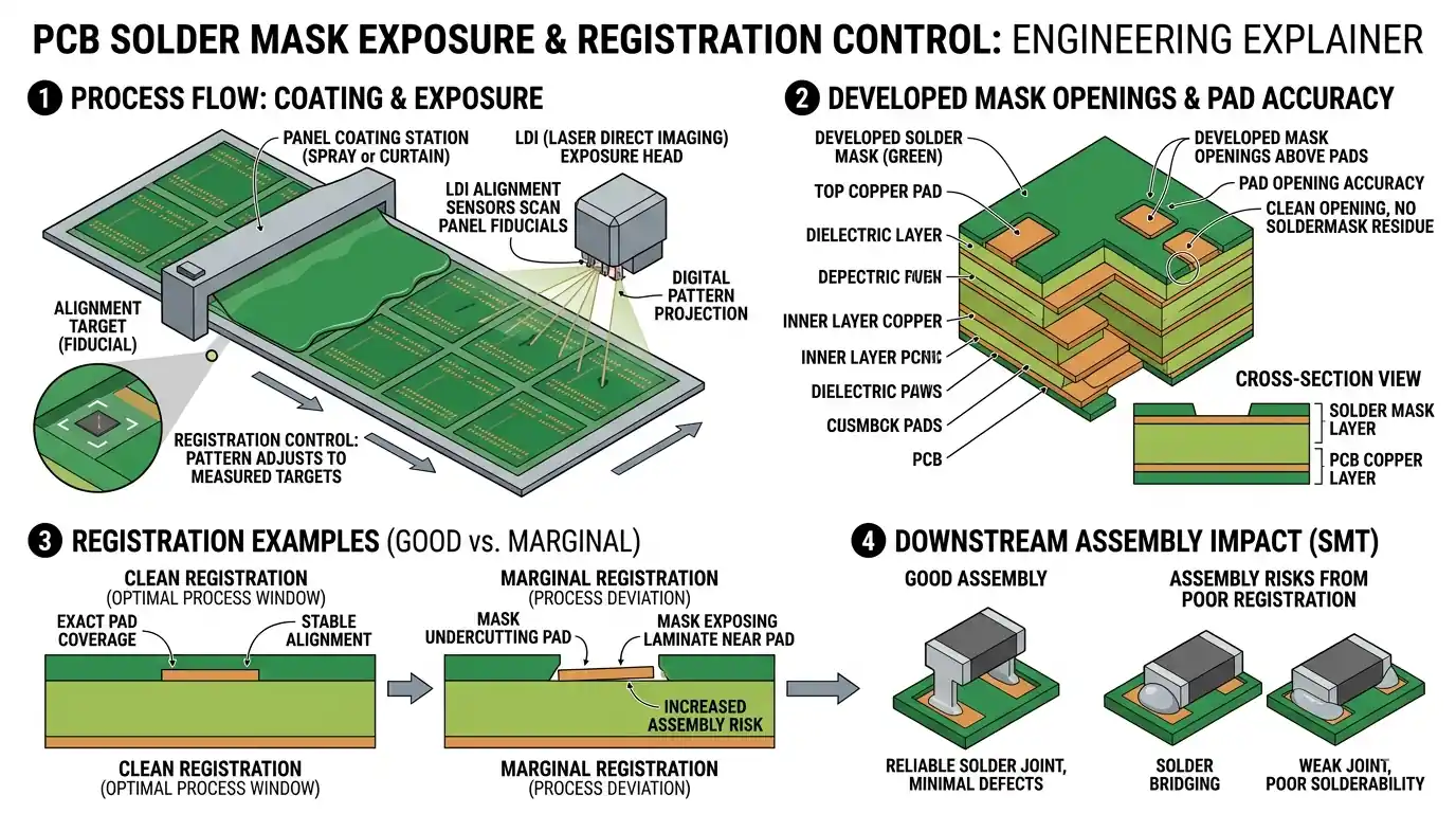
The soldermask layer is not just a cosmetic coating. It protects exposed copper, defines pad-opening boundaries, and directly affects assembly yield and long-term reliability. When soldermask exposure control is unstable, a board may still pass electrical test, yet show bridging, poor solder wetting, difficult rework, and weak lot-to-lot consistency during assembly.
For sourcing teams and hardware engineers, soldermask exposure should not be treated as just another PCB shop step. It should be treated as part of the factory's core process capability. Alignment accuracy, development window, curing stability, and inspection traceability all directly affect whether prototype and volume production will deliver the same result.
Why soldermask exposure affects downstream yield
The exposure step decides which areas keep soldermask and which pads or vias remain open. That directly affects:
- whether soldermask dams between fine-pitch pads stay stable enough
- whether pad edges are encroached by ink
- whether tented vias remain fully covered
- adhesion after reflow, cleaning, and environmental stress
- cosmetic and dimensional consistency across production lots
If the process window is too narrow, even small shifts in exposure energy, panel positioning, or development time can later expand into assembly defects.
LDI and film exposure do not fit the same kinds of designs
Traditional film exposure can still work well on standard boards, but once pad pitch tightens and alignment tolerance becomes smaller, control difficulty rises quickly. Film stretch, handling error, and panel movement all increase soldermask offset risk.
These situations usually justify LDI:
- fine-pitch BGA or QFN
- very narrow soldermask dams
- HDI dense-pad regions
- designs with already limited annular-ring margin
- RF boards or medical boards that need strong repeatability and dimensional stability
The key question is not which imaging method sounds more advanced. It is whether the factory chooses the right method for the board's real geometry.
Alignment and process window drive most downstream risk
Many soldermask problems only show up during SMT, but their root cause often sits in unstable exposure and development control. A mature PCB factory should be able to explain clearly how it controls:
- panel positioning before imaging
- exposure energy for different ink systems and board thicknesses
- development speed and residue removal
- final curing profile and adhesion verification
- ongoing lot-to-lot consistency, not just a one-time good sample
Once these factors drift, pad residue, weak soldermask edges, exposed copper at trace boundaries, or opening sizes that no longer match the design become much more likely.
The defect types engineering teams should really watch
When evaluating a PCB supplier, the real issue is not whether it can apply soldermask at all. The issue is whether it can avoid the critical failure modes consistently. Common examples include:
- soldermask misregistration that reduces pad spacing or exposes copper at trace edges
- underexposure, leaving weak opening boundaries and poor adhesion
- overexposure, shrinking small openings and thinning fine soldermask dams
- development residue on pad surfaces, which later hurts solderability
- tented vias cracking or breaking open after thermal stress
- soldermask encroachment onto pads, especially around fine-pitch components
These are not just cosmetic defects. They often lead to solder bridging, uneven wetting, unstable test behavior, and higher rework cost.
Design-side DFM directly affects soldermask yield
Many soldermask issues do not come from the PCB shop alone. They come from design files that leave too little manufacturing margin. During DFM review, a few checks deserve close attention:
- whether soldermask dam width matches the target factory's stable production capability
- whether pad spacing leaves enough room for alignment variation
- whether annular-ring loss after drilling weakens soldermask support
- whether a via should be tented, plugged, or left open, and whether that matches the cleaning and assembly plan
- whether silkscreen sits too close to pads or soldermask openings
- whether the chosen surface finish is compatible with the soldermask system and reflow profile
For industrial control, automotive electronics, medical, and telecom products especially, these issues cannot be judged only by saying the bare board "looks fine."
Soldermask quality should be judged together with assembly behavior
Soldermask process quality should not be judged only at the bare-board stage. The more useful question is whether it stays stable through paste printing, placement, reflow, selective soldering, cleaning, and rework.
For example:
- weak-adhesion soldermask is more likely to peel during rework
- unstable opening boundaries can affect stencil release and solder-joint shape
- unstable via tenting may crack after thermal cycling or trap contamination
- inconsistent copper exposure on pads can change solder-joint appearance from lot to lot on the same design
That is why mature PCB suppliers do not separate soldermask from downstream assembly feedback. They feed assembly results back into front-end process control.
Inspection and traceability decide whether a factory stays stable over time
Soldermask exposure is one of those processes where visual appearance alone is not enough. The factory needs a repeatable method to confirm alignment, opening quality, adhesion, and cure result, instead of relying only on operator experience.
Useful control points commonly include:
- AOI or optical checks on critical opening regions
- alignment verification through sample panels or test areas
- adhesion or tape testing when needed
- defect-trend tracking by lot, panel, and equipment condition
- traceability linking ink batch, exposure settings, and production date
If a program is expected to move from prototype into repeated volume production, these capabilities become especially important. A reliable supplier should be able to explain how it keeps the process under control over time, not just show one attractive panel.
What to confirm with the PCB factory before release
If your product is sensitive to soldermask quality, it is usually more useful to ask specific questions than to ask only for a minimum soldermask dam number. Good questions include:
- which imaging method will be used for this board, and why
- what the stable production minimum soldermask dam really is
- how soldermask alignment is verified in dense-pad regions
- whether vias in this design are better tented, plugged, or left open
- how pad residue and contamination risk are controlled before surface finish and assembly
- which process parameters remain traceable if one lot later shows adhesion or alignment problems
The more specific the answers, the more likely the supplier is evaluating your design as a volume product instead of just mechanically processing a Gerber file.
FAQ
Why does soldermask exposure affect SMT yield?
Because it directly defines pad-opening boundaries, soldermask dam stability, and whether pads are encroached. Even small variation in exposure or development can later become solder bridging, uneven wetting, or difficult rework.
Should fine-pitch boards always use LDI first?
Often yes, but the answer still depends on pad spacing, soldermask dam width, and the factory's real production capability. The key is not the equipment name but whether alignment and repeatability stay stable.
If the bare board looks normal, does that prove the soldermask process is fine?
No. Soldermask quality also depends on adhesion, post-reflow behavior, rework durability, and lot consistency. Many problems only appear after the board enters assembly.
What is the most common soldermask-related DFM issue on the design side?
Typical issues include soldermask dams that are too narrow, pad spacing that is too tight, via treatment that does not match the assembly flow, and silkscreen placed too close to openings.
What is most worth confirming with the board shop before release?
First confirm the imaging method, the stable production minimum soldermask dam, the alignment verification method, the via tenting or opening strategy, and the traceability plan for abnormal lots.
Conclusion
PCB soldermask exposure is not a minor cosmetic step. It is a manufacturing process directly tied to yield and reliability. Imaging method, alignment control, development window, curing stability, and design margin all influence whether the soldermask system can support downstream assembly consistently.
For dense designs and high-reliability products, it is better to confirm soldermask rules and process window with the manufacturer early in the design cycle. That is how soldermask exposure becomes a controlled manufacturing step instead of a hidden defect source in volume production.