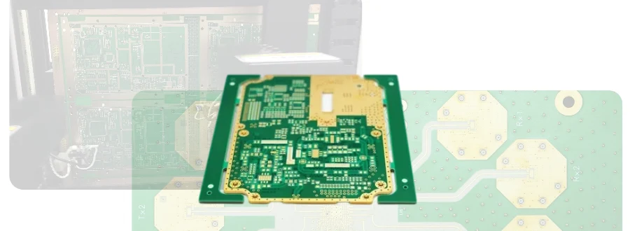
Why Choose Highleap PCB Factory for RF PCB Manufacturing?
With over 15 years of expertise in RF and microwave PCB production, Highleap PCB Factory delivers precision-engineered circuit boards for demanding wireless applications. Our advanced manufacturing capabilities and rigorous quality controls ensure optimal performance for your RF designs—from prototype to high-volume production.
Our RF PCB Manufacturing Capabilities
- Frequencies up to 77 GHz for 5G and radar applications
- Rogers, Taconic, and other high-frequency materials
- Precise impedance control (±5% tolerance)
- Advanced via structures including blind/buried vias
- Comprehensive RF testing and validation
- Full RF PCB assembly services
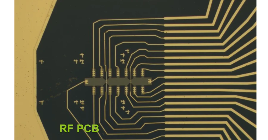
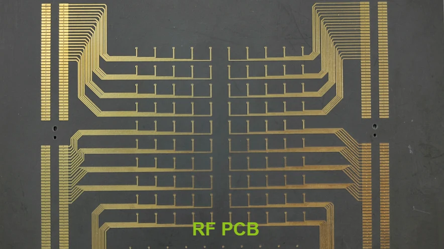
RF PCB Manufacturing Specifications
Supporting advanced RF applications
Precise controlled impedance
High-precision RF traces
Designing RF PCBs requires a deep understanding of both the manufacturing process and the factors that influence performance, cost, and manufacturability. Here are some best practices to follow for optimizing RF PCB designs, improving production efficiency, and reducing costs.
1. Designing for Manufacturability (DFM)
Ensuring that your design is easy to manufacture can significantly reduce production costs and increase efficiency. The key considerations for DFM in RF PCB manufacturing include:
- Simplify Circuit Design and Layout: Avoid overly complex circuit designs and unnecessary components. Simplifying the design reduces manufacturing complexity, lowers costs, and accelerates production.
- Minimize Trace Lengths: Longer traces can lead to increased signal loss and potential signal integrity issues. Keeping trace lengths short and well-planned helps reduce noise and improves signal quality.
- Impedance Matching: Proper impedance matching is crucial for maintaining signal integrity. Pay attention to trace width and spacing to ensure consistent impedance and avoid reflections and signal degradation【Learn more about RF PCB impedance control】(/blog/rf-pcb-impedance-control).
2. Material Selection and Handling
Choosing the right materials is critical for RF PCB performance, as they impact signal integrity, thermal management, and manufacturability.
- Select the Right High-Frequency Materials: Materials such as Rogers, Taconic, and Isola offer excellent dielectric properties that minimize signal loss. Ensure the material chosen matches your design’s performance requirements for high-frequency applications【Learn more about RF PCB materials】(/blog/rf-pcb-materials).
- Thermal Management: RF PCBs often operate in high-temperature environments. Choose materials with good thermal conductivity to improve heat dissipation and prevent overheating of components during operation.
- Cost Optimization: While high-performance materials are essential for optimal performance, balance the cost of materials with the required specifications. Consider the performance-to-cost ratio to ensure that materials meet your technical requirements without unnecessary expense.
3. Advanced Manufacturing Techniques
RF PCB manufacturing requires precision at every step to ensure quality and performance. Optimizing the manufacturing process can help reduce production costs and increase reliability.
- High-Precision Imaging and Etching: RF designs often require fine features, such as narrow traces, which need high-resolution etching and imaging to ensure accuracy. This improves signal quality and the overall performance of the PCB.
- Layer-to-Layer Registration: Tight layer registration is crucial for multi-layer RF designs to avoid misalignment of vias and traces, which can lead to signal interference. Ensuring precise alignment improves overall board reliability.
- Blind and Buried Vias: Using blind and buried vias can reduce signal interference, improve signal paths, and help reduce board space usage. This technique is particularly beneficial in complex multi-layer designs, helping to cut costs and save space【Learn more about RF PCB assembly】(/blog/rf-pcb-assembly).
4. Effective Testing and Quality Control
Thorough testing and quality control are essential to ensure that RF PCBs perform as expected. Here’s how to optimize testing to avoid costly errors and improve the quality of the final product:
- Impedance Testing with Network Analyzers: Impedance mismatch can lead to signal reflections and reduced performance. Use network analyzers to measure impedance across traces and vias, ensuring they meet design specifications.
- Signal Integrity Testing: Use signal integrity tests to identify any issues related to signal loss, reflection, or crosstalk. Early detection of these issues can help make adjustments before moving to mass production【Learn more about RF PCB testing】(/blog/rf-pcb-testing).
- Automated Optical Inspection (AOI): AOI systems can quickly detect manufacturing defects such as misalignment, missing components, or soldering issues, improving production speed and reducing human error.
5. Cost Optimization Strategies
Reducing production costs without compromising on performance is essential for staying competitive in the market. Here’s how to optimize costs in RF PCB manufacturing:
- Use Standardized Materials and Components: Select off-the-shelf components and standardized materials where possible to reduce costs. Custom parts and rare materials can significantly increase the price of production.
- Prototype and Testing in Phases: By prototyping the design and performing testing in phases, you can catch any issues early on. This minimizes the risk of costly errors in mass production.
- Reduce Layer Count: While multi-layer designs are sometimes necessary for complex RF PCBs, simplifying the design and reducing the number of layers can lower both material and manufacturing costs.
By following these best practices, you can ensure that your RF PCB designs are optimized for manufacturability, performance, and cost-effectiveness. This approach will help you maintain high standards of quality while also improving production efficiency and reducing costs.
How to Choose the Right Testing Methods for RF PCBs
Selecting the right testing methods for RF PCBs is crucial to ensure high performance and reliability. By focusing on key factors like impedance, signal integrity, and thermal management, you can optimize your RF PCB design for real-world applications.
- Impedance Testing: Use network analyzers to measure impedance across transmission lines. TDR (Time Domain Reflectometry) can help pinpoint mismatches that could cause signal degradation or reflection.
- Signal Integrity Testing: Eye pattern testing is ideal for evaluating high-speed signal quality, while crosstalk testing ensures minimal interference between adjacent signal traces, which is essential for high-density designs.
- Thermal Testing: Perform thermal cycling tests to assess durability under temperature changes, and use infrared thermography to monitor heat distribution and identify potential hotspots.
At Highleap PCB Factory, we offer more than just high-quality RF PCB manufacturing and assembly. We provide expert guidance on stack-up design, impedance control, and recommend the best RF materials for your specific application. Let us help optimize your RF designs with reliable and cost-effective solutions. Contact us today to learn more about how we can support your RF PCB needs.
Cost-Effective Approaches for Scaling RF PCB Production
Scaling RF PCB production while keeping costs under control is a significant challenge for many businesses. The goal is to increase production volume without sacrificing quality or performance. Here are practical, cost-effective approaches that can help you scale RF PCB production efficiently:
- Material Selection with Mixed-Press Technology: One effective way to reduce costs is by using mixed-press materials. By combining high-frequency materials with lower-cost substrates, you can achieve a balanced performance at a more affordable price point. For example, using a combination of Rogers material for high-frequency areas and standard FR4 for other layers can lower costs without compromising critical performance areas. This mixed approach allows for greater flexibility in material selection, helping meet both performance requirements and budget constraints. For more information on high-frequency materials, see our article on High-Frequency PCB.
- Design for Manufacturability (DFM) and Layer Optimization: Simplifying PCB designs by reducing unnecessary layers and components is a key cost-saving strategy. By leveraging DFM reviews, designers can ensure that their RF PCBs are optimized for the manufacturing process. This can involve adjusting layer stack-ups, optimizing routing to minimize trace lengths, and reducing the use of complex via structures. These small adjustments can lower production costs significantly without sacrificing signal integrity or performance.
- Panelization and Efficient Space Utilization: Maximizing the use of PCB panel space is essential for reducing material waste and lowering overall costs. Panelization involves arranging multiple PCB designs on a single panel to optimize the space used during manufacturing. This approach minimizes the material wasted during production and reduces costs per unit. Efficient layout techniques can also help reduce the need for larger boards, which in turn lowers material and handling costs.
- Automated Assembly and Testing: Automation plays a key role in scaling RF PCB production cost-effectively. The use of pick-and-place machines for component assembly and automated optical inspection (AOI) for quality control helps reduce labor costs, minimize human error, and increase throughput. Automated testing methods, such as in-circuit testing (ICT) and functional testing, ensure that each board meets performance requirements while speeding up the production process, allowing for faster scaling at a lower cost.
- Batch Production and Prototyping to Reduce Waste: Instead of moving directly from prototype to large-scale production, start with small batch runs. This allows for testing and validation of designs at lower volumes, identifying potential issues before committing to larger quantities. Prototyping helps reduce costly rework during high-volume production, ensuring that only fully validated designs are scaled, which prevents financial losses from faulty products.
- Supply Chain and Bulk Procurement: Another strategy for cost-effective scaling is supply chain optimization. Consolidating suppliers for materials, components, and assembly services can reduce procurement costs through bulk purchases and negotiated discounts. Strong supplier relationships also help with consistent material quality and lead times, ensuring that production schedules are met without delays or price hikes.
- Outsourcing and Subcontracting: For non-critical tasks, consider outsourcing certain aspects of production to specialized manufacturers. Subcontracting assembly or testing processes can help lower operational costs, especially when scaling production quickly. This also allows your internal team to focus on design and other high-priority tasks, while external partners handle the labor-intensive production aspects.
By implementing these strategies, you can scale your RF PCB production efficiently while keeping costs under control. At Highleap PCB Factory, we provide expert guidance on material selection, DFM, and automation to help you achieve a balance between cost efficiency and high-quality RF PCB manufacturing. We also offer specialized insights on Microwave PCBs and other RF solutions. Contact us today to discuss how we can help optimize your RF PCB production process.
Conclusion
At Highleap PCB Factory, we are committed to providing high-quality RF and microwave PCB manufacturing solutions that meet the demands of today’s advanced wireless applications. With over 15 years of experience, we offer precision-engineered circuit boards designed for optimal performance, whether you are developing solutions for 5G, radar, IoT, or satellite communications.
From custom stack-up designs to impedance control, RF material recommendations, and full PCB assembly services, we provide a comprehensive range of solutions that ensure your RF PCBs are optimized for performance, cost-efficiency, and scalability. Whether you are prototyping or scaling to mass production, we are here to support your needs and help you navigate the complexities of RF PCB design and manufacturing.
Reach out to us today to discuss your RF PCB requirements and discover how Highleap PCB Factory can deliver the reliable, high-performance solutions you need to bring your innovations to life.