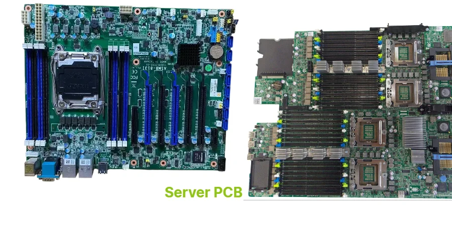
Server PCBs demand exceptional performance standards for data centers, cloud infrastructure, and enterprise computing. Highleap PCB Factory (HILPCB) manufactures and assembles these complex boards—from compute motherboards to storage backplanes and riser cards—with a disciplined focus on signal integrity, power delivery, and thermal management. Our engineers understand the challenges of high-speed differential pairs, dense BGA breakouts, and multilayer stackups that today's server hardware demands.
Server PCB Core Requirements and Design Priorities
Modern server boards must handle ever-increasing data rates while maintaining reliability and serviceability:
High-speed interfaces: PCIe Gen4/5/6, DDR4/5, multi-GbE to 400G Ethernet, and coherent links requiring tightly matched differential pairs, length/phase control, and minimized via stubs through blind/buried or back-drilled strategies. For lanes above 10+ Gbps, our high-speed PCB techniques ensure consistent impedance and minimal loss.
Multilayer architecture: Typical server boards require 10–24+ layers with stable reference planes and optimal stackup design. Our multilayer PCB manufacturing handles complex stackups with varied dielectric thicknesses and copper weights.
Material selection: High-Tg laminates for thermal margin and low-loss materials for critical signal paths. Many server designs combine standard FR-4 materials with selective low-Dk/Df layers where signal loss budgets are tightest.
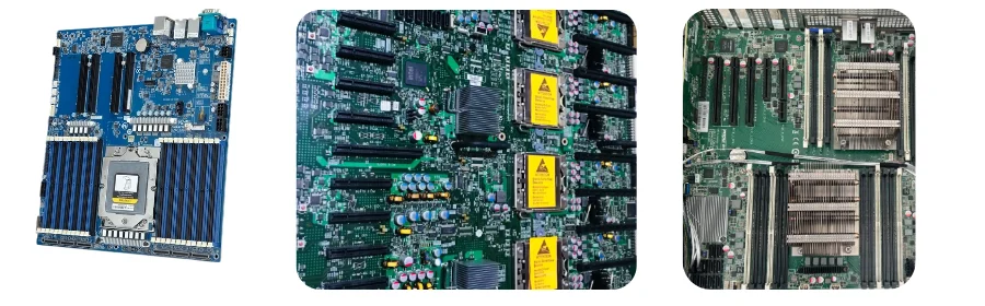
Server peripherals: Complete ecosystem boards including backplanes, risers, BMC/management modules, mezzanine cards, and OCP-compliant interconnects. Our specialized backplane PCB production handles the long formats and heavy connector loads these applications demand.
Pro tip: Define your stackup early in development. Use test coupons and an accurate impedance table, and validate with pre-production TDR measurements before layout freeze to avoid expensive re-spins.
Materials, Stackups, and Manufacturability Considerations
Material selection represents the foundation of successful server PCB performance. High-speed server designs begin with high-Tg FR-4 as a baseline substrate, providing thermal stability during reflow and long-term reliability in data center environments. When insertion loss budgets become critical—particularly for long PCIe runs or 100G links—selective application of low-loss dielectrics on outer signal layers delivers substantial performance improvements while maintaining cost control. Keeping core materials consistent simplifies lamination processes and minimizes warpage during thermal cycling.
Copper distribution throughout the stackup plays a crucial role in both electrical and mechanical performance. Power planes and connector pads typically utilize 1 oz copper for current handling and mechanical stability, while signal layers benefit from 0.5 oz copper to enable finer geometries and tighter impedance control. Balanced copper weighting across the entire stackup prevents warping during assembly processes, a particularly important consideration for larger server boards with numerous BGA components and press-fit connectors that demand exceptional flatness.
Via structures require careful planning in server PCB designs to enable both high performance and manufacturing feasibility. Laser microvias provide optimal breakout paths from dense BGA regions, while back-drilling techniques eliminate performance-robbing stubs from long through-vias in high-speed channels. Surface finish selection—typically ENIG or immersion silver—ensures both planarity for fine-pitch components and corrosion resistance for high-cycle connector interfaces. Our online impedance calculator helps designers align their transmission line targets with manufacturing capabilities for optimal first-pass success.
Assembly, Test, and Reliability
Server PCB assembly requires precision placement, controlled reflow profiles, and comprehensive testing to ensure reliable field performance:
Advanced assembly: Our processes handle fine-pitch BGA components, high-mass power modules, press-fit connector cages, and precision edge connectors through our sophisticated SMT assembly equipment and expertise.
Comprehensive testing: We implement AOI, X-ray inspection for hidden joints, boundary scan where available, and functional power-on validation including voltage rail verification, DDR training, and PCIe link establishment.
Thermal verification: During pilot runs, we profile thermal performance with infrared imaging and in-situ temperature logging to identify and address any hotspots before volume production.
Reliability assessment: HALT-style accelerated testing and connector insertion cycle validation ensure your server boards will perform reliably throughout their service life.
Best practice: Always conduct a pilot build with limited panels to validate reflow profiles, connector planarity, and thermal distribution before committing to volume production.
Cost, Lead Time, and Documentation Requirements
Understanding the key cost drivers helps optimize server PCB designs for performance and value:
Primary cost factors: Layer count, percentage of low-loss materials, via technology complexity (stacked microvias/back-drilling), panelization efficiency for long boards, and yield-affecting tolerance requirements.
Typical lead times: Prototypes 10–14 business days; production runs 3–5 weeks depending on stackup complexity, lamination cycles, and test coverage.
Documentation essentials: Comprehensive fabrication notes with finish specifications, thickness requirements, impedance tables, back-drill maps, press-fit specifications, gold-finger requirements, and acceptance criteria. Use our Gerber viewer during DFM review to identify potential manufacturing issues.
Strategic approach: Maintain consistent "golden" stackups across server product families (mainboards, backplanes, risers) to improve material purchasing efficiency and reduce lamination setup variations.
Why HILPCB for Server PCB Projects
Proven high-speed expertise: Successful track record with PCIe Gen4/5/6, DDR4/5, 25G/100G Ethernet, and other high-performance interconnects.
Material optimization: We help you determine where premium low-loss materials deliver value—and where standard FR-4 remains sufficient—ensuring performance margins without unnecessary cost.
Quality at scale: From pilot runs through volume production, we maintain consistent inspection standards and test protocols.
Engineering collaboration: We provide stackup recommendations, SI/PI guidance, and practical design feedback during DFM review—preventing surprises at first-article inspection.
Frequently Asked Questions
What Server PCB types do you build?
We manufacture mainboards, storage/compute backplanes, riser and mezzanine cards, BMC/management PCBs, and I/O interface boards—each with impedance control and connector-specific requirements.Which materials should I choose for high-speed links?
Start with high-Tg FR-4 plus low-loss dielectric on critical layers; use premium materials only where loss budgets demand it. Our high-speed PCB engineering team can help determine the optimal material mix.How do you control impedance and skew risk?
We implement early stackup verification, coupon testing, and precise geometry control. Symmetric glass styles and controlled lamination processes minimize skew. Use our impedance calculator and consult with our engineers before finalizing layouts.Can you handle long backplanes with heavy connectors?
Yes, we specialize in manufacturing and assembling long-format backplane PCB designs with fixtured connector alignment and staged reflow processes.What assembly and inspection coverage do you provide?
Our SMT assembly capabilities include fine-pitch BGA and press-fit components with AOI, X-ray inspection, boundary scan testing (when supported), and comprehensive power-on validation.What are typical prototype and production lead times?
Prototypes typically require 10–14 business days. Production runs average 3–5 weeks depending on stackup complexity, drilling strategy, and test requirements.How can I reduce Server PCB costs without compromising performance?
Consolidate stackups across product lines, limit premium low-loss materials to the specific layers that require them, and avoid unnecessarily tight tolerances. Early collaboration with our multilayer PCB team during DFM review typically identifies significant cost-saving opportunities.