
Multilayer PCB Services & PCB Stackup Planning | 4–64 Layers, Backdrill & Impedance Control
Prototype-to-production multilayer PCB services and PCB stackup planning for 4–64 layer builds, with stackup review, backdrill planning, sequential lamination, stacked microvias, and impedance control ±5%. Registration typically ±15–25 μm.
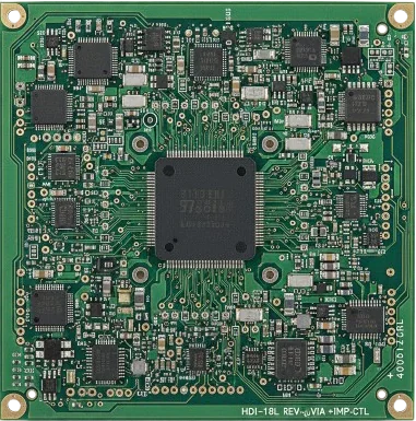
Multilayer PCB Stackup Architecture & Registration Precision
Optical/X-ray alignment for reliable high-layer buildsHigh-layer-count designs demand stackups that balance signal integrity, power distribution and manufacturability. Our engineering team correlates field-solver simulations with controlled-impedance stackups and test coupons to maintain differential targets at 85/90/100 Ω within ±5%. Optical registration and X-ray targets achieve layer-to-layer alignment typically within ±15–25 µm, protecting via reliability beyond 20 layers.
Material options range from standard FR-4 to low-loss systems for high-speed PCB channels. Hybrid stackups place premium dielectrics only where needed, often cutting material cost by 30–50% while preserving SI. For dense interconnects, HDI PCB architectures with any-layer microvias reduce layer count without sacrificing performance. This multilayer PCB service path is used from early prototypes through later production releases so the approved stackup can continue without re-framing the build.
Critical Risk: Inconsistent dielectric flow or asymmetric lamination can create Z-axis CTE stress, resin-starved voids, or conductive-anodic-filament (CAF) growth between layers—common failure points in multilayer boards above 16–20 layers.
Our Solution: We employ lamination process control with press-cycle monitoring, resin-flow SPC, and vacuum debubbling to ensure uniform dielectric fill. Each build is validated with TMA expansion data and cross-section inspection to confirm Z-axis reliability. Stackup symmetry and copper balancing minimize warpage, while signal-integrity modeling aligns impedance and loss predictions with measured coupon data.
For mission-critical systems—telecom backplanes, defense or automotive control units—our Backplane PCB platforms extend multilayer reliability to 40-plus layers with controlled resin cure profiles and press-fit tolerance validation. Explore additional thermal and mechanical guidance in thermal management in PCB design.
- Layer counts up to 64
- Registration accuracy typically ±15–25 μm
- Microvia aspect ratio below 1:1
- Impedance tolerance ±5% achievable
- CAF mitigation and resin systems with Td >340 °C
- Warpage control typically <0.75%
🚀 Quick Quote Request
📋 Get Full Capabilities
Sequential Lamination & Via Technologies
Multi-stage build-up with comprehensive process verificationSequential lamination enables routing densities unreachable with conventional builds. Each cycle uses staged pressure/temperature with resin flow typically 10–20% to stabilize dielectric thickness for impedance. UV-laser microvias commonly 75–125 μm are depth-controlled within ±5 μm and desmeared for clean metallization. Via fills include non-conductive resin (planarized ±5 μm) or copper fill for ~10× thermal/electrical conduction in power paths—see advanced via technologies.
Inline AOI detects inner-layer features down to 25 μm; X-ray verifies registration; TDR on coupons validates impedance before release. IST (Interconnect Stress Test) cycling typically 200–500 checks robustness; microsections confirm ≥20 μm barrel copper. For long-reach backplanes, coordinate with backplane PCB teams on backdrill and connector strategy.
- Microvia diameter 75–125 μm common
- Copper-filled microvias for 10× thermal gain
- IST 200–500 cycles
- Minimum barrel copper 20 μm
- Ionic contamination ≤1.56 μg/cm²
- Process Cpk typically ≥1.33
Multilayer & HDI PCB Technical Specifications
Comprehensive capabilities for complex high-speed/high-density designs
| Parameter | Standard Capability | Advanced Capability | Standard |
|---|---|---|---|
Layer Count | 4–12 layers | Up to 64 layers | IPC-2221 |
Base Materials | FR-4 Tg 150–180 °C | Megtron/Rogers/Isola low-loss | IPC-4101 |
Board Thickness | 0.6–3.2 mm | Up to 8.0 mm | IPC-A-600 |
Copper Weight | 0.5–2 oz (17–70 μm) | Up to 4 oz | IPC-4562 |
Min Trace/Space | 75/75 μm (3/3 mil) | 25/25 μm (1/1 mil) | IPC-2221 |
Min Hole Size | 0.15 mm (6 mil) mechanical | 0.05 mm (2 mil) laser | IPC-2222 |
Via Technology | Through-hole, blind/buried | Microvias, stacked vias, via-in-pad | IPC-6012 |
Max Panel Size | 571.5 × 609.6 mm | 571.5 × 1200 mm | Manufacturing capability |
Impedance Control | ±10% | ±5% | IPC-2141 |
Surface Finish | ENIG, OSP, Immersion Silver | ENEPIG, Hard/Soft Gold | IPC-4552/4556 |
Quality Testing | 100% E-test, AOI | Impedance (TDR), X-ray, microsection | IPC-9252 |
Certifications | ISO 9001, UL, RoHS/REACH | IATF 16949, AS9100, ISO 13485 | Industry standards |
Lead Time | 5–7 days | 3 days express | Production schedule |
Need capabilities beyond this product? Explore our full manufacturing capabilities
Ready to start your PCB project?
Whether you need simple prototypes or complex production runs, our advanced manufacturing capabilities ensure excellent quality and reliability. Get your quote within 30 minutes.
Signal Integrity Design & Via Strategy
Maintain differential-pair spacing ~2× trace width and place ground-via fences within ~1× via diameter for return-path continuity above 1 GHz. Backdrill residual stubs to <10 mil for links beyond 10 Gbps. Power-plane splits must preserve return currents; the classic 20H rule can reduce edge radiation for EMC. Our DFM review validates these before release.
- Dk/Df stability checks across −40 to +125 °C
- Via-stub resonance screening above 5 GHz
- Thermal relief for heavy-copper planes
- ICT access targeting ≥95%
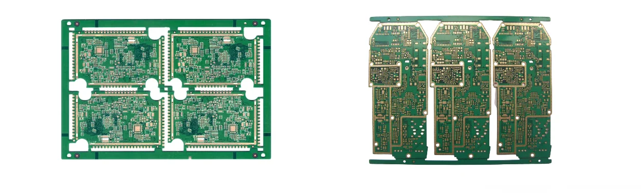
Complete Process Flow with Quality Gates
Inner layers image to 75 μm standard and 25 μm advanced. AOI covers 100% of inner layers; lamination employs vacuum presses reaching 185–195 °C with staged pressure to prevent resin starvation. Post-lamination X-ray confirms ±15–25 μm registration. Mechanical drilling uses 300k RPM class spindles; plating builds 25–35 μm in barrels. For HDI iterations, lamination/drill cycles repeat with metrology at every stage.
Testing includes flying-probe/fixture E-test, TDR impedance correlation, microsections and IST. Data is tied to lot travelers and retained for 7–10 years for automotive/aerospace programs. For system-level builds and enclosures, see box build assembly.
Impedance Control with Field-Verified Modeling
Edge coupons undergo TDR with ±2 Ω typical accuracy to validate solver predictions. Standard FR-4 Df ~0.015–0.020 at 1 GHz vs low-loss 0.002–0.005 extends channel reach. Smooth copper (Rz <2 μm) improves insertion loss ~10–20% above 5 GHz. See our impedance control method and high-speed co-design with high-speed PCB.
Reliability Validation & SPC Monitoring
Thermal cycling −40↔+125 °C for 500–1000 cycles with resistance drift <10%. HAST 130 °C/85% RH screens moisture risks; SIR confirms ≥10^8 Ω. SPC tracks registration, hole position, plating thickness and impedance; first articles verify dimensions typically ±0.05 mm and impedance within ±5%.
Application-Specific Implementation Strategies
Telecom/Datacom: 24–32 layers with low-loss dielectrics and backdrill for 25+ Gbps.
Aerospace/Defense: IPC Class 3 documentation and extended lot retention.
Industrial/Power: 2–4 oz planes; pair with heavy copper PCB as needed. For long-reach chassis, coordinate with backplane PCB.
Engineering Assurance & Certifications
Experience: volume multilayer/HDI builds with registration typically ±15–25 μm and coupon-verified impedance.
Expertise: sequential lamination, microvia fill, backdrill control and Cpk ≥1.33.
Authoritativeness: built to IPC-6012 Class 3; see IPC Class 3 notes.
Trustworthiness: MES traceability (lot to unit level) with TDR/IST/microsection reports available on request.
- Controls: resin flow, dielectric thickness, drill registration
- Traceability: digital traveler and lot reports
- Validation: TDR, IST, cross-sections, ionic and SIR
Frequently Asked Questions
How many layers can you reliably manufacture?
Which via options are recommended for high speed?
How is impedance verified in production?
Which materials should I choose for 10–28+ Gbps?
Do you support box-level builds after fabrication?
Experience Advanced PCB Manufacturing Excellence
From simple prototypes to complex production runs, our world-class factory delivers superior quality, fast turnaround and competitive pricing. Join thousands of satisfied customers who trust us with their PCB manufacturing needs.