
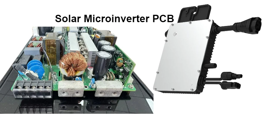
PCB солнечного микроинвертора — это силовая и управляющая платформа для преобразования энергии одного или нескольких PV-модулей в согласованный с сетью переменный ток. Плата реализует часть MPPT, преобразования, измерения, защиты, связи и диагностики, но не подтверждает сама по себе безопасность изделия, anti-islanding, сетевое соответствие или ресурс установленной системы.
Микроинвертор отличается от центрального или строкового инвертора не только мощностью. Он работает непосредственно у модуля, обычно в компактном наружном корпусе, с ограниченным пассивным охлаждением и сложным сервисом. Поэтому топология, изоляция, силовые контуры, тепловой путь, potting, enclosure и производственный тест должны проектироваться как одна система.
Для инженера результатом должна быть связка «электрический corner → конструкция → измерение → критерий приемки». Для NPI — контролируемая конфигурация и failure coverage. Для закупок — предложение с одинаковыми материалами, BOM, fixtures, испытаниями и ответственностью.
Ключевые выводы
- Сначала зафиксируйте PV input window, output/grid configuration, topology, isolation concept, power states, communication и target markets; слово «microinverter» не определяет плату.
- Разделяйте PV-side, DC link, gate drive, bridge, AC filter/grid interface, control, sensing и communications по энергии, изоляции и fault containment.
- Creepage/clearance нельзя выбирать по одной номинальной величине напряжения: нужны рабочие и переходные напряжения, категория, загрязнение, материал, высота, coating/potting и применимые требования изделия.
- Минимизируйте критичные switching/gate loops и измеряйте их поведение на representative power stage; общий совет «короткие широкие дорожки» недостаточен.
- Тепловой путь проходит от junction через package, solder, copper/vias, interface material, potting и enclosure. Высокий Tg не заменяет расчет и корреляцию.
- Potting или coating меняет тепло, влажность, partial-discharge/insulation behavior, rework и inspection; процесс должен быть частью released design.
- AOI/X-ray/ICT/FCT/hi-pot закрывают разные дефекты. Они не доказывают inverter efficiency, anti-islanding или grid compliance.
- EVT/DVT/PVT/FAI должны контролировать hardware, BOM, magnetics, firmware, calibration, enclosure, potting, fixture и limits как одну baseline.
- В RFQ отдельно указывайте lab/product certification, которые выполняет владелец изделия, и board/PCBA evidence, которое поставляет изготовитель.
Содержание
- Какие блоки входят в микроинвертор?
- Какие design inputs нужно заморозить?
- Как определить изоляцию, creepage и clearance?
- Как выпускать switching loops, gate drive и sensing?
- Как связать MPPT, управление и grid interface?
- Как построить тепловой путь?
- Когда применять coating или potting?
- Какие материалы и stack-up нужны?
- Как обеспечить DFM, DFA и DFT?
- Как связать отказ и доказательство?
- Что доказывает каждый уровень испытаний?
- Какие gate нужны от EVT до PVT?
- Как управлять BOM и изменениями?
- Как сравнивать поставщиков, стоимость и срок?
- Что включить в RFQ?
- Где заканчивается область HILPCB?
- Практические вопросы
Какие блоки входят в микроинвертор?
Архитектуру нужно описывать через energy path и protection states. Конкретная топология может быть изолированной или неизолированной, одно- или многоступенчатой; supplier PCB не должен угадывать ее по назначению изделия.
| Блок | Функция | Критичные входы | Evidence |
|---|---|---|---|
| PV input | соединение модуля, protection, current/voltage sensing | voltage/current window, reverse/transient states и connector | input sweep, protection reaction и thermal |
| MPPT/DC-DC | согласование рабочей точки и преобразование | topology, switching, magnetics, control range | efficiency/loss breakdown, loop behavior и corner |
| DC link | накопление энергии и decoupling | ripple, capacitor current, precharge/discharge | ripple/temp, discharge state и component stress |
| DC-AC bridge | формирование AC current/voltage | switches, gate drive, dead time, current sense | waveform, loss, protection и fault injection |
| Filter/grid interface | filtering, relay/contactor, sensing и connection | grid variants, surge/EMC, isolation и disconnect | conducted/EMC, relay state и product tests |
| Control/comms | timing, MPPT, diagnostics, gateway link | firmware, clocks, isolation, update и fail-safe state | checksum, logs, update/recovery и communication |
Широкий обзор инверторной электроники находится в руководстве по inverter PCB. Здесь акцент на плате, которая постоянно находится у PV-модуля и должна сохранять electrical, thermal и environmental margin в компактном корпусе.
Какие design inputs нужно заморозить?
Номинальная мощность — только одна строка. Рабочая таблица должна включать:
| Категория | Входные данные | Почему влияет на PCB |
|---|---|---|
| PV source | voltage/current window, module count, cold/open-circuit and hot/low-light corners | напряжение, ток, MPPT range и protection |
| Grid/output | voltage/frequency variants, current, power factor, fault and disconnect states | switch stress, filter, relay, sensing и test variants |
| Topology | isolation, stages, switching frequency, magnetics and control method | domains, loops, creepage, heat и layer use |
| Environment | module-back temperature, solar heating, humidity, condensation, altitude and mounting | material, clearance, enclosure и thermal path |
| Lifetime/service | mission profile, cycling, no-service or repair policy, warranty assumptions | derating, component choice, potting и traceability |
| Evidence | PCB/PCBA tests, product safety/EMC/grid tests, raw data and owners | test points, fixture и acceptance boundaries |
Каждый числовой limit должен иметь operating state, tolerance, measuring point и owner. Не переносите рабочую температуру PV-модуля напрямую на junction limit силового ключа или на Tg ламината.
Как определить изоляцию, creepage и clearance?
Изоляционная таблица строится по всем доменам и переходным состояниям, а не по одному сетевому напряжению. В ней фиксируют basic/reinforced или другую требуемую функцию, working/transient voltage, pollution/material assumptions, altitude, coating/potting treatment, barrier components и test method.
| Граница | Что зафиксировать | PCB/PCBA проверка |
|---|---|---|
| PV to low-voltage control | topology, transformer/opto/digital isolator, slots and return path | drawing audit, dimensional inspection, hi-pot/insulation scope |
| Grid to control/comms | relay/sensing/isolation, connector and protective earth concept | creepage/clearance record, component identity, functional reaction |
| Primary-secondary magnetics | winding construction, bobbin/core, PCB pads and solder | supplier report, incoming identity and product verification |
| Adjacent HV nets | max differential/transient, contamination and coating | spacing/slot inspection, process record and sample test |
Hi-pot без specified ramp, dwell, limit, discharge и test nodes неполон. Успешный PCBA test не заменяет safety construction review готового корпуса и не доказывает anti-islanding.
Как выпускать switching loops, gate drive и sensing?
Критичный loop описывают геометрией, током, dv/dt или di/dt, return path и measurement point.
| Контур | Главный риск | Что проверить |
|---|---|---|
| Input decoupling-switch | overshoot, EMI и switch stress | loop area, package/decoupling placement, probe method |
| Gate drive | false turn-on, ringing, common-source inductance | gate loop, Kelvin path, resistor/driver location и waveform |
| Bridge/DC link | bus inductance, capacitor RMS current и heat | copper/layer path, capacitor placement and thermal corner |
| Current sense | common-mode transient, noise, offset and delay | Kelvin sense, isolation, filter, calibration and fault range |
| Snubber/clamp | energy, tolerance, temperature and failure mode | waveform before/after, component stress and production identity |
В release package сохраняют схемы петель, layout screenshot, stack-up, model assumptions, oscilloscope setup и representative waveform. Это полезнее общей фразы «EMC-oriented layout».
Как связать MPPT, управление и grid interface?
MPPT, current control, synchronization и protection используют одни датчики, clocks и силовой тракт, но имеют разные критерии. Плата должна обеспечивать integrity измерений и outputs; алгоритмы и сетевые функции принадлежат владельцу firmware/product.
| Функция | PCB input | System evidence |
|---|---|---|
| MPPT | voltage/current sensing accuracy, sampling, noise and calibration | response over PV curves and conditions |
| Current control | ADC/PWM timing, gate path, dead time and current feedback | waveform, stability, distortion and fault reaction |
| Grid sensing | voltage/frequency path, isolation, zero crossing/timebase | accuracy, phase/timing and abnormal-grid response |
| Disconnect/protection | relay/driver, feedback, discharge and safe state | stuck/open/contact cases and end-to-end response |
| Monitoring | energy/sensor data, timestamp, communication and update | data consistency, diagnostics and fleet/gateway integration |
Подробный алгоритмический контекст оставлен странице MPPT controller board. Для supplier acceptance важны измеримый analog path, calibration record, programmed firmware и reaction to faults.
Как построить тепловой путь?
Thermal design — это сеть сопротивлений и источников потерь от junction до внешней среды. Разделите conduction, switching, magnetics, capacitor ESR, relay/contact и control losses по operating corner.
| Участок | Design input | Корреляция |
|---|---|---|
| Junction-package | loss model, package, solder and exposed pad | electrical loss estimate + temperature measurement |
| PCB spreading | copper area/weight, vias, planes, isolation constraints | board model, coupon/cross-section where needed |
| Interface | gap pad, pressure, flatness, insulation and aging | assembly control and contact-area inspection |
| Potting/enclosure | conductivity, cure, voids, CTE, wall and mounting | material lot/process, CT/X-ray/sample section if justified |
| Ambient | module-back condition, sun/wind, orientation and thermal cycling | chamber/outdoor profile and installed comparison |
Высокий Tg помогает пережить часть thermal/process нагрузки, но не снижает junction temperature автоматически. Высокотеплопроводная PCB или толстая медь выбирается после loss map и isolation constraints.
Когда применять coating или potting?
Защитный материал выбирают по failure mode и service policy. Он может снизить риск влаги и поддержать механически компоненты, но усложняет void control, rework, failure analysis и heat flow.
| Решение | Преимущество | Риск/контроль |
|---|---|---|
| Conformal coating | локальная влагозащита, меньшая масса, возможный rework | coverage, bubbles, keep-outs, adhesion and inspection |
| Partial potting | защита выбранных power/magnetic zones | interface, stress gradient, contamination and repair boundary |
| Full potting | environmental/mechanical encapsulation and heat path | cure exotherm, voids, CTE stress, no-service policy and disposal |
| Sealed enclosure only | serviceability and simpler FA | gasket/vent/condensation, connector and pressure cycling |
Укажите chemistry, supplier, mix/cure, preconditioning, dispensing, void criteria, keep-outs, adhesion, repair и batch traceability. Замена compound требует impact assessment по теплу, изоляции, механике и process window.
Какие материалы и stack-up нужны?
Stack-up должен одновременно выполнять power, isolation, thermal, control и manufacturing requirements.
- определите copper weight и geometry из current/temperature rise и manufacturability;
- задайте dielectric thickness по isolation, capacitance и thermal path;
- разделите noisy switch nodes, gate/control, sensing и communications с контролируемыми return paths;
- проверьте copper balance, warpage и mixed SMT/THT assembly;
- укажите laminate/foil/finish exact identity и правила alternates;
- согласуйте coating/potting adhesion и reflow/selective-solder process.
Число слоев не является качеством. Иногда дополнительный слой улучшает return/thermal spread; иногда увеличивает capacitance across isolation или стоимость без пользы. Решение подтверждают review и measurement.
Как обеспечить DFM, DFA и DFT?
| Риск | Design input | Production evidence |
|---|---|---|
| HV spacing/slots | domain drawing, routing, mask/coating and tolerances | AOI/dimensional rule and sample record |
| Power package void/open | land, stencil, thermal pad, reflow and heat sinking | SPI/AOI/X-ray criteria and reaction |
| THT magnetics/connectors | hole/pad, mass, support and solder method | selective/wave profile, fill criteria and pull/visual sample |
| High-current nets | copper/via/terminal and resistance limit | electrical resistance, cross-section if specified |
| Programming/calibration | firmware, serial, keys/config and calibration constants | checksum, read-back, genealogy and lock |
| Potting/coating | keep-out, cleanliness, cure, void and batch | process log, visual/weight/section plan |
Test points не должны нарушать isolation или добавлять паразитный loop. Fixture design следует начать до layout freeze, особенно для high-voltage functional test, safe discharge и programmed calibration.
Как связать отказ и доказательство?
| Симптом | Возможные причины | Метод изоляции | Owner/evidence |
|---|---|---|---|
| switch overshoot/ringing | loop inductance, gate path, probe, package or snubber | correct probing, layout/model review and A-B parts | power design |
| thermal shutdown | loss, interface void, enclosure contact, potting or sensor | loss map, IR/thermocouple, section and thermal replay | thermal/NPI |
| insulation fail | spacing, contamination, material, void, damage or component | visual/dimensional, hi-pot/IR, section and genealogy | safety/supplier quality |
| EMI fail | switch node, common-mode path, cable, filter or enclosure | near-field/current probe, conducted/radiated A-B | EMC/system |
| low conversion performance | switching/conduction/magnetic loss, control or measurement | power analyzer, waveform and calibration audit | power/control |
| field intermittent | moisture, solder fatigue, connector, thermal cycling or firmware | environmental reproduction, FA and configuration log | product/quality |
Failure analysis должна сохранять first-fail condition и as-received configuration. Rework до фиксации waveform, insulation или thermal evidence может уничтожить причину.
Что доказывает каждый уровень испытаний?
| Уровень | Доказательство | Не доказывает |
|---|---|---|
| Bare PCB | construction, electrical continuity, dimensions, stack-up and selected coupons | converter function or insulation of all components |
| PCBA inspection/electrical | assembly, programming, rails, sensors, switching and agreed insulation/FCT | final enclosure, grid or anti-islanding acceptance |
| Power-stage bench | waveform, loss, thermal, protection and corner behavior | outdoor life or market conformity |
| Finished product | enclosure/potting, environmental, EMC/safety/grid functions | performance of every PV installation |
| PV-system monitoring | installed energy/availability and sensor data per defined method | root cause at PCB without diagnostics |
IEC 61724-1 helps define PV-system performance monitoring, but it is not a PCB manufacturing standard. Product safety, EMC, grid connection and installation requirements must be mapped separately by market and product owner.
Какие gate нужны от EVT до PVT?
| Gate | Что закрыть | Выходной пакет |
|---|---|---|
| EVT | topology, sensing, gate loops, bring-up, protection and initial thermal | waveforms, rework, risk register and next revision |
| DVT | representative stack-up/BOM/enclosure/potting, electrical/environment/EMC/safety plan | requirement matrix, corner data and issue closure |
| PVT | production panel, assembly, programming, calibration, potting and EOL | FAI, yield/defects, correlation, genealogy and control plan |
| Release/change | approved baseline, deviation and re-validation scope | signed record, raw evidence, PCN/EOL and disposition |
Более широкий процесс описан в руководстве EVT/DVT/PVT для inverter. Для микроинвертора особенно важно, чтобы PVT применял production-equivalent enclosure и potting process.
Как управлять BOM и изменениями?
Baseline связывает PCB revision и stack-up, BOM/AVL, magnetics construction, power-semiconductor lot/revision, firmware, calibration, enclosure, TIM, potting/coating, fixture, scripts, limits и raw results.
Для alternate проверяйте switching/thermal loss, gate charge, capacitance, isolation, magnetic saturation/loss, capacitor ripple/life, relay/contact behavior, sensor offset, package/land и firmware impact. Совпадение номинала или корпуса не доказывает эквивалентность.
Как сравнивать поставщиков, стоимость и срок?
| Критерий | Что запросить | Как сравнить |
|---|---|---|
| PCB | exact stack-up/material/copper/finish, slots, tolerances and tests | одинаковая released construction |
| Assembly | power packages, magnetics/THT, reflow/selective solder, coating/potting | одинаковый process и acceptance |
| Test | fixture, safe discharge, programming, calibration, FCT/hi-pot, raw data | одинаковые nodes, limits and sample rate |
| Sourcing | AVL, alternates, traceability, MOQ/NCNR, EOL and storage | одинаковые approval rules |
| Quality | FAI, first fail, MRB, rework, FA, retention and PCN | одинаковые deliverables and response |
Стоимость и срок определяют power semiconductors, magnetics, capacitors/relays, copper/stack-up, mixed assembly, fixtures, programming/calibration, potting/coating, enclosure, safety/EMC/grid lab work, sample count и component availability. Разделяйте unit price, NRE, materials commitment и external lab cost.
Что включить в RFQ микроинвертора?
- PV input, output/grid variants, topology, isolation concept, power states, target markets and installation profile.
- Schematic, layout, ODB++/Gerber, drill/slots, stack-up, impedance if applicable, fabrication/assembly drawings and panel intent.
- BOM/AVL with exact power devices, magnetics, capacitors, relays, sensors, connectors, firmware-programmable parts and alternate rules.
- Electrical limit table: working/transient voltages, currents, switching states, protection, creepage/clearance domains and safe discharge.
- Thermal package: loss budget, junction/case/board/enclosure points, TIM, potting/coating, ambient profiles and acceptance.
- Gate/switching/current-sense models, critical-loop drawings, probing reference and representative waveform limits.
- Enclosure, connector, cable, grounding/earth, vent/gasket, mounting and potting drawings/process.
- DFM/DFA/DFT, SPI/AOI/X-ray/ICT/FCT/hi-pot scope, fixture, calibration, limits, raw data and failure reaction.
- EVT/DVT/PVT/FAI quantities, configuration, genealogy, packaging, storage and environmental/product lab responsibilities.
- Commercial terms: NRE/tooling/fixtures, unit-price breaks, MOQ/NCNR, excess, lead-time basis, PCN/EOL, FA/corrective action, assumptions and exclusions.
Закупочный контекст дополнен страницей solar PCB procurement. Сравнивайте предложения на одной revision и требуйте список assumptions отдельно.
Где заканчивается область HILPCB?
После проверки файлов HILPCB может оценить изготовление PCB и смешанную сборку: поверхностный монтаж управляющих и силовых компонентов, а также монтаж выводных деталей для согласованных магнитных компонентов и разъемов. Sourcing, DFM/DFT, programming и electrical/functional tests включаются только как явно описанные deliverables; stack-up, copper, coating/potting, fixture и hi-pot/FCT подтверждаются в quotation.
Владелец микроинвертора отвечает за topology/control, safety architecture, anti-islanding, grid/EMC/product conformity, enclosure and installed PV performance, если эти deliverables не включены отдельно. Успешная PCBA приемка — необходимый производственный уровень, но не разрешение на подключение к сети.
Практические вопросы
Чем PCB микроинвертора отличается от платы строкового инвертора?
Она обычно обслуживает меньше PV-модулей, работает непосредственно у модуля, имеет компактный пассивно охлаждаемый корпус и иной service model. Но topology, voltage domains и grid requirements все равно задаются конкретным изделием.
Всегда ли микроинвертор должен иметь гальваническую изоляцию?
Нет универсального ответа. Это архитектурное решение, зависящее от topology, product safety, market, grounding и system requirements. Supplier должен получить утвержденную isolation matrix, а не выбирать ее самостоятельно.
Как определить creepage и clearance?
По working/transient voltages, insulation function, pollution/material assumptions, altitude, coating/potting и применимым требованиям изделия. Значения должны быть выпущены safety authority и проверяемы на drawing/assembly.
Достаточно ли использовать high-Tg laminate?
Нет. Tg не определяет junction temperature, thermal resistance, isolation, moisture behavior или lifetime. Нужны loss map, stack-up, copper/vias, interface, enclosure и thermal correlation.
Когда нужна толстая медь?
Когда current profile, geometry, allowable temperature rise, vias, terminals и thermal path это обосновывают. Она может усложнить etch, assembly и isolation, поэтому выбирается по расчету и process evidence.
Potting всегда повышает надежность?
Он может улучшить влагозащиту и механическую поддержку, но способен создать voids, CTE stress, cure heat, difficult rework и новый thermal path. Надежность подтверждается на выбранном compound и процессе.
Что должен измерять FCT?
Rails, boot, programmed revision, sensors, switching/drive states, protection, communication и согласованные output conditions. FCT должен иметь безопасную fixture, limits, raw data и first-fail policy.
Hi-pot подтверждает сетевое соответствие микроинвертора?
Нет. Он проверяет определенную insulation path при заданных test conditions. Grid behavior, anti-islanding, EMC, enclosure и product safety требуют отдельных испытаний и владельцев.
Как проверять gate-drive layout?
Зафиксировать critical loop, Kelvin return, driver/resistor location, probe method и representative load/corner. Оценивать gate waveform, false turn-on, ringing, overshoot и component stress.
Какие изменения требуют повторной валидации?
Stack-up, copper, power switch, driver, magnetics, capacitor, relay, sensor, firmware, TIM, potting, enclosure, fixture или limit. Impact assessment определяет затронутые electrical, thermal, EMC, insulation и product tests.
Что должен доказать PVT?
Что production materials, line, soldering, programming, calibration, potting, fixtures, limits, traceability и reaction plan совместно воспроизводят approved design. Нужны first-pass yield и first-fail data, а не только shipped quantity.
Как сравнить два коммерческих предложения?
Использовать одинаковые stack-up, BOM/AVL, alternates, assembly, potting, fixtures, test, raw data, quantities, NRE и lab responsibilities. Сверять assumptions, MOQ/NCNR, excess и lead-time basis.
Какие файлы ускоряют точный RFQ?
Architecture/limits, schematic/layout, stack-up, BOM/AVL, isolation matrix, thermal package, enclosure/potting, firmware/calibration, DFM/DFT, test nodes/limits, NPI quantities, deliverables and change rules.