
Performance testing validates that high frequency PCBs meet their electrical specifications and will function correctly in the target application. At microwave frequencies, standard continuity and isolation tests reveal only basic connectivity—they cannot detect impedance variations, excessive loss, or signal integrity problems that cause circuit failures. Comprehensive HF testing requires specialized equipment, methodologies, and acceptance criteria that address the unique challenges of high frequency signal propagation.
This guide provides complete knowledge of HF PCB performance testing, from fundamental measurement principles through practical test strategies that ensure your boards meet demanding high frequency requirements.
HILPCB provides RF circuit board manufacturing with comprehensive testing capabilities including TDR impedance verification, VNA characterization to 67 GHz, and detailed test reporting for complete performance validation.
In this article:
- Why HF PCB Testing Differs From Standard Testing
- Essential Test Equipment for HF Verification
- Impedance Testing and TDR Analysis
- S-Parameter and Network Analysis
- Test Coupon Design and Placement
- Test Data Interpretation and Acceptance
Why HF PCB Testing Differs From Standard Testing
Standard PCB testing—continuity, isolation, and basic electrical verification—cannot assess high frequency performance. The tests that matter at HF involve parameters invisible to DC measurements.
At HILPCB, our precision PCB manufacturing includes HF-specific testing that goes far beyond standard electrical verification.
Frequency-Dependent Behavior
PCB characteristics change with frequency. Impedance that measures correctly at DC may vary significantly at operating frequency. Loss mechanisms that are negligible at low frequency become dominant at GHz frequencies. Coupling between traces that doesn't exist at DC creates crosstalk at high frequency. Testing must occur at or near the actual operating frequency to reveal real performance.
Distributed Element Effects
At high frequencies, every trace is a transmission line with distributed inductance and capacitance. Reflections occur at impedance discontinuities. Standing waves affect signal amplitude along trace length. These effects don't exist at DC and require time-domain or frequency-domain analysis to detect.
Signal Integrity Parameters
HF testing addresses parameters standard testing ignores: characteristic impedance and its variation along trace length, insertion loss and its frequency dependence, return loss indicating reflection magnitude, crosstalk between adjacent signals, and propagation delay and skew. Each parameter requires specific measurement techniques and equipment.
Manufacturing Correlation
Test results must correlate with manufacturing parameters. Impedance variation indicates trace width or dielectric thickness problems. Excessive loss suggests roughness or material issues. This correlation enables process improvement when test results fall outside specifications. Understanding signal testing for high frequency PCB fundamentals supports effective manufacturing feedback.
Essential Test Equipment for HF Verification
Proper equipment enables accurate HF measurements. Understanding equipment capabilities guides test strategy development.
Time Domain Reflectometer (TDR)
TDR is the primary tool for impedance verification. It sends a fast-rise-time pulse down the trace and measures reflections. Reflection timing indicates discontinuity location; reflection magnitude indicates impedance deviation.
Key TDR specifications include rise time (determines spatial resolution—faster is better), system impedance (typically 50Ω), dynamic range (ability to measure small reflections), and time window (maximum trace length measurable).
Modern TDR systems achieve sub-50 ps rise times, enabling inch-level resolution. HILPCB uses precision TDR for 100% impedance testing on controlled impedance boards.
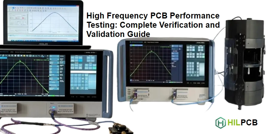
Vector Network Analyzer (VNA)
VNA measures S-parameters—the complete frequency-domain characterization of a network. S11 (return loss) indicates reflection; S21 (insertion loss) indicates transmission loss; S12 and S22 complete the two-port characterization.
Key VNA specifications include frequency range (must cover operating frequency), dynamic range (ability to measure high-loss paths), port count (for multi-port devices), and calibration quality (determines measurement accuracy).
HILPCB provides VNA testing to 67 GHz for demanding PTFE board verification and millimeter-wave applications.
HILPCB HF Testing Capabilities
Spectrum Analyzer
Spectrum analyzers measure signal amplitude versus frequency. Useful for EMI pre-compliance, spurious signal detection, and harmonic analysis. Not typically used for PCB acceptance testing but valuable for system-level debugging.
Oscilloscope with HF Capability
High-bandwidth oscilloscopes (multi-GHz) enable time-domain signal viewing. Essential for eye diagram analysis in high-speed digital applications. Jitter measurement and signal quality assessment require adequate oscilloscope bandwidth.
Impedance Testing and TDR Analysis
Impedance testing verifies that controlled impedance traces meet their target values. TDR provides both average impedance and impedance profile along trace length.
Detailed methodology: Transmission Analysis for HF PCB
TDR Measurement Principle
TDR sends a step signal into the trace. At any impedance change, part of the signal reflects back. The time delay between transmitted and reflected signals indicates the distance to the discontinuity. The reflection coefficient indicates the impedance deviation.
For a reflection coefficient ρ: Z_actual = Z_system × (1 + ρ)/(1 - ρ)
Coupon-Based Testing
Production impedance testing uses test coupons—dedicated structures on the panel designed specifically for testing. Coupons include launch structures compatible with test probes, trace geometries matching production traces, and lengths adequate for meaningful measurement.
Testing coupons rather than production circuits avoids the difficulty of probing actual circuit features while providing representative data.
Interpreting TDR Results
TDR traces show impedance versus distance. Look for average impedance relative to target, impedance variations along trace length, discontinuities at transitions (via, connector), and launch quality (initial impedance step).
Acceptable results show smooth impedance within tolerance band. Problem indicators include oscillations (probe contact issues), systematic offset (geometry or material error), and local discontinuities (manufacturing defects).
Differential Impedance Testing
Differential pairs require testing in differential mode. The TDR sends complementary signals on both traces and measures differential impedance. This tests both the impedance and the pair balance simultaneously. Imbalanced pairs show as impedance variation even if individual traces are correct.
S-Parameter and Network Analysis
S-parameters provide complete frequency-domain characterization. VNA measurements reveal performance across the full frequency range of interest.
Detailed methodology: Frequency Response Testing for PCB
S-Parameter Fundamentals
For a two-port network, four S-parameters describe behavior: S11 (input reflection coefficient or return loss), S21 (forward transmission coefficient or insertion loss), S12 (reverse transmission coefficient), and S22 (output reflection coefficient).
For passive reciprocal networks (most PCB structures), S12 = S21.
Return Loss (S11)
Return loss measures how much signal reflects at the input. Higher return loss (more negative in dB) means less reflection. For 50Ω systems, typical requirements are S11 < -10 dB (good), S11 < -15 dB (better), and S11 < -20 dB (excellent).
Return loss varies with frequency, often degrading at higher frequencies where small discontinuities become electrically significant.
Insertion Loss (S21)
Insertion loss measures signal attenuation through the structure. It includes conductor loss, dielectric loss, and radiation loss. Insertion loss increases with frequency—specify loss at the maximum operating frequency.
For PCB traces, insertion loss of 0.5-2 dB per inch at 10 GHz is typical depending on material and geometry.
Mixed-Mode S-Parameters
For differential pairs, convert single-ended S-parameters to mixed-mode parameters: Sdd (differential-to-differential), Scc (common-to-common), Sdc (differential-to-common, mode conversion), and Scd (common-to-differential, mode conversion).
Mode conversion parameters indicate pair balance. Well-balanced pairs have low Sdc and Scd. This analysis is critical for high-speed differential interfaces.
Test Coupon Design and Placement
Test coupons enable efficient, accurate testing without probing production circuits. Proper coupon design ensures test results represent actual circuit performance.
Coupon Types
Standard coupon types include single-ended microstrip and stripline, differential pairs (edge-coupled and broadside), impedance discontinuities (via transitions), and loss measurement structures.
Select coupon types matching your critical circuit structures. Include all controlled impedance trace types used in the design.
Geometric Matching
Coupons must match production trace geometry: same trace width and spacing, same dielectric thickness, same copper weight, and same layer positions.
If geometry differs, coupon results don't represent circuit performance. Use design rules to ensure coupons match circuits.
Launch Design
The probe-to-coupon interface (launch) must not limit measurement quality. Use ground-signal-ground (GSG) or ground-signal-signal-ground (GSSG) patterns matching probe pitch. Include adequate ground around signal pads. Taper from pad to trace if dimensions differ.
Poor launches create reflections that mask true trace performance.
Placement Strategy
Position coupons to represent panel variation. Include coupons at panel center and corners. Multiple coupons reveal process uniformity. Place coupons where they won't be removed before testing. Coupon placement relates to overall high frequency board validation strategy.
Test Data Interpretation and Acceptance
Raw test data requires interpretation to determine pass/fail status and guide process improvement.
Specification Comparison
Compare measured values against specifications. Impedance: typically ±5% or ±10% of target. Loss: maximum dB/inch at specified frequency. Return loss: minimum dB at operating frequency.
Clear specifications enable objective pass/fail decisions.
Statistical Analysis
Analyze data statistically across production. Calculate mean, standard deviation, and Cpk. Track trends over time. Identify systematic variations versus random variation.
Statistical analysis reveals process capability beyond individual pass/fail results. This supports process improvement for HF PCB debugging and manufacturing optimization.
Correlation with Design
Compare test results with design predictions. Simulation should predict measured impedance, loss, and other parameters. Correlation validates both design models and manufacturing process.
Discrepancies indicate either modeling errors or process variations that need investigation.
Report Generation
Document test results for traceability. Include coupon identification and location, test equipment and calibration status, measured values with pass/fail indication, and graphical data (TDR traces, S-parameter plots).
Complete documentation supports quality system requirements and enables future reference.
HILPCB provides comprehensive test reports for Rogers high-frequency laminate and other HF board production.
HILPCB HF Testing Services
HILPCB delivers comprehensive testing for high frequency PCBs:
Impedance Verification: 100% TDR testing on controlled impedance with detailed reporting.
VNA Characterization: S-parameter measurement to 67 GHz for millimeter-wave applications.
Custom Test Development: Test strategies tailored to your specific requirements and frequency range.
Data Analysis: Statistical analysis and trend tracking for process optimization.
From RF prototypes through volume production, HILPCB provides testing that validates high frequency performance.
Contact HILPCB for HF testing consultation and manufacturing quotation.
Common Questions
Why isn't TDR alone enough for high-frequency PCB performance testing?
TDR is excellent for locating impedance discontinuities, but it does not tell the full story about insertion loss, return loss, or broadband channel behavior. Once frequencies rise and the design margin shrinks, teams usually need both time-domain and frequency-domain data.
When should a VNA be brought into the test plan?
A VNA becomes important when the design has to validate S-parameters, channel loss, connector transitions, or behavior deep into the operating band. For RF, microwave, and millimeter-wave work, it is often the tool that confirms whether the assembled signal path really matches the model.
Why do test coupons have to match the real production geometry so closely?
Because coupon results are only meaningful when the trace width, spacing, dielectric thickness, copper weight, and layer location reflect the actual circuit. If the coupon geometry drifts away from the product geometry, the measurements stop representing the hardware you are trying to qualify.
What should engineers focus on when reviewing high-frequency production test reports?
They should look beyond simple pass or fail and check the measured values against the design target, statistical spread, coupon location, calibration status, and correlation with simulation. A useful report explains whether the process is under control, not just whether one board passed.