
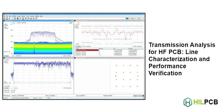
HF PCB transmission analysis is the measured characterization of impedance, reflection, insertion loss, phase, delay and mode conversion through a defined interconnect and between defined reference planes. It turns a stackup or channel model into evidence that engineering and manufacturing teams can use for design correlation and production release.
Key Takeaways
- Write a measurement contract before selecting an instrument: define the DUT, reference planes, ports, bandwidth, state, limits and required evidence.
- TDR/TDT localizes discontinuities in time or distance; a VNA directly measures complex S-parameters over frequency. Either can support transformed-domain analysis when configured correctly.
- Calibration moves the measurement plane to a known interface. Port extension, time gating and de-embedding are different operations and are not interchangeable.
- Differential channels need port mapping, polarity, reference impedance and mixed-mode terms—not only a differential impedance number.
- A coupon represents a product channel only when material, layer, geometry, processing and launch relationships are controlled.
- Use repeatability, uncertainty and guard bands when setting acceptance limits; a visually smooth trace is not a release criterion.
Table of Contents
- Define the Measurement Contract
- Choose TDR, TDT or VNA
- Measure Impedance and Locate Discontinuities
- Measure Loss, Phase and Delay
- Analyze Differential and Mixed-Mode Behavior
- Calibrate, Remove Fixtures and Validate Data
- Design Representative Test Coupons
- Use a Transmission Analysis Release Matrix
- Diagnose Common Measurement Failures
- HF PCB Transmission Analysis RFQ Checklist
- Reference Standards and Responsibility Boundaries
- How HILPCB Supports Measurable Interconnects
- FAQ
- Conclusion
Define the Measurement Contract
“Test the impedance” is incomplete. The same coupon can produce different-looking results when rise time, bandwidth, window, reference impedance, launch removal or distance conversion changes. Freeze the following before layout release:
| Contract item | Required definition | Why it matters |
|---|---|---|
| DUT | Coupon, bare-board route, connectorized channel or assembled link | Determines whether launches, vias and connectors belong in the result |
| Reference planes | Physical interfaces where the DUT begins and ends | Prevents fixture loss or mismatch from being assigned to the PCB |
| Ports | Numbering, polarity, single-ended/differential mapping and terminations | Required for repeatable mixed-mode conversion |
| Frequency/time range | Start/stop frequency, points, IF bandwidth or TDR step response | Sets observable loss, delay and spatial detail |
| Operating state | Bare/assembled, bias, temperature, cables and termination | Makes results comparable across samples and laboratories |
| Metrics | Z0, S11/S21, Sdd, Scd/Sdc, phase, group delay or crosstalk | Links the test to the actual channel risk |
| Decision rule | Limit, evaluation band, averaging, uncertainty and guard band | Converts plots into an objective pass/fail record |
Set the upper frequency from the interface spectrum, edge rate, compliance method and model use—not nominal clock alone. Define the Touchstone reference impedance and required raw, calibrated and de-embedded files.
Choose TDR, TDT or VNA
The instruments overlap, but their strongest evidence differs.
| Method | Best evidence | Main cautions |
|---|---|---|
| TDR | Reflection versus time; impedance profile; location of opens, shorts and local discontinuities | Apparent detail depends on incident step, system response, launch and filtering |
| TDT | Transmitted step/impulse response and time-of-flight | Requires a defined receive plane and appropriate termination |
| VNA | Complex reflection and transmission S-parameters versus frequency | Calibration, dynamic range, cables, connectors and fixture removal control accuracy |
| VNA time transform | Frequency-correlated location of reflection events and optional gating | Resolution and unambiguous range depend on sweep settings and windowing |
| EM/channel simulation | Pre-layout prediction and sensitivity analysis | Accuracy is limited by geometry, material models, roughness and boundary assumptions |
TDR/TDT data can support network models, and VNA sweeps can be transformed into time-domain views. Correlation requires aligned bandwidth, reference planes, normalization and fixture treatment.
Measure Impedance and Locate Discontinuities
Characteristic impedance follows the distributed transmission-line parameters:
Z0 = sqrt((R + jωL) / (G + jωC))
The lossless sqrt(L/C) approximation omits frequency-dependent conductor, dielectric and roughness effects. Production impedance also depends on finished geometry, dielectric thickness, effective Dk, copper profile, solder mask and reference planes.
A TDR converts reflection coefficient to an impedance profile. Positive and negative excursions can indicate higher and lower local impedance. Because the waveform includes the measurement-system response, a narrow via or pad may not appear as its physical shape.
Do not infer universal spatial resolution from rise time alone. Propagation velocity, system response, bandwidth, noise, launch and filtering affect what can be separated. Record the applied setting.
Measure Loss, Phase and Delay
For a two-port interconnect, S11 describes input reflection and S21 forward transmission at stated reference planes. A per-unit-length loss result is valid only after separating launch/fixture contributions and measuring length consistently.
Loss includes copper/roughness, dielectric, geometry, return discontinuities, radiation, launches and resonances. Multiple line lengths or a suitable removal structure can help separate line loss from launch loss.
Unwrap phase consistently before deriving delay. Group delay comes from the frequency derivative of transmission phase and becomes unreliable near the noise floor or a deep notch. Report it only over a valid magnitude region.
Propagation velocity depends on effective permittivity and field distribution, so microstrip and stripline can differ. Use measured length and delay when timing margin matters.
Analyze Differential and Mixed-Mode Behavior
A differential pair is a four-port network before mathematical conversion. Confirm connector orientation, P/N polarity and port order before generating mixed-mode S-parameters.
| Evidence | Engineering question |
|---|---|
| Differential TDR / odd-mode impedance | Is the coupled pair near its target along the route? |
| Sdd11 | How much differential energy reflects at the input? |
| Sdd21 | How much differential signal transmits, including loss and dispersion? |
| Scd/Sdc terms | How much energy converts between differential and common modes? |
| Pair skew / phase balance | Are the two conductors electrically symmetric enough for the interface? |
| Near/far-end crosstalk | Does an aggressor couple excessive energy into another path? |
There is no universal mode-conversion or skew limit; the interface, receiver, EMI objective and band set it. Pad/via asymmetry, glass weave, reference transitions, connector fields and unequal returns can create conversion despite length matching.
Calibrate, Remove Fixtures and Validate Data
Calibration corrects systematic errors and establishes reference planes using a suitable method such as SOLT or TRL. It does not automatically remove every launch before the product channel.
Port extension can compensate line delay/loss but not generally fixture mismatch. Time gating suppresses selected responses and alters frequency data. De-embedding removes a characterized fixture network; quality depends on its model, topology, bandwidth and conditioning.
Before accepting a de-embedded file, check:
- expected low-frequency continuity and plausible high-frequency behavior;
- causality and passivity for a passive DUT;
- reciprocity only when the physical network should be reciprocal;
- smooth phase, correct port mapping and consistent reference impedance;
- sensitivity to reconnection, cable movement, calibration age and fixture model;
- agreement between raw and processed data around known launch events.
Processed data can look cleaner while becoming less physical. Preserve raw data, fixture files, settings and software version.
Design Representative Test Coupons
A coupon is a process monitor, not automatically a product-channel surrogate. Match production layer, dielectric, copper/roughness, finished geometry, mask, reference planes, via treatment and fabrication flow. Use panel locations that reveal meaningful variation.
TDR coupons need enough uniform line to identify a stable region. Loss extraction may use multiple lengths or a through structure for the chosen removal method. Differential fixtures need symmetric, repeatable launches.
Do not default to 3–6 inches. Choose length so the measured effect exceeds uncertainty without entering the noise floor, and confirm coupon-to-product process correlation.
Use a Transmission Analysis Release Matrix
This matrix binds each claim to a measurement plane and releasable evidence.
| Release gate | Controlled inputs | Evidence | Reject or investigate when |
|---|---|---|---|
| Pre-layout | Interface band, stackup, loss/impedance budget and topology | Field-solver/channel model plus assumptions | Material or geometry cannot meet margin across tolerance |
| Coupon design | Layer, process, launches, lengths and removal method | Coupon-to-product correlation map | Coupon omits the product's dominant construction variable |
| Lab setup | Instrument, calibration, cables, torque, ports and environment | Setup record and verification standard | Reference plane or port map is ambiguous |
| Prototype | Production-intent board and assembly state | Raw plus processed TDR/VNA data and model correlation | Failure changes materially with reconnection or processing choice |
| Production | Lot/panel sampling and fixed test recipe | Statistical results with uncertainty/guard band | Drift, outlier pattern or coupon/product correlation breaks |
| Change control | Material, stackup, artwork, process, fixture or software revision | Impact review and targeted requalification | Prior evidence no longer represents the released configuration |
Diagnose Common Measurement Failures
| Symptom | Likely cause | Discriminating check |
|---|---|---|
| TDR ripple changes between connections | Launch contact, cable movement or insufficient settling | Repeat connects against a verification line |
| Loss improves unrealistically after removal | Incorrect fixture orientation, port map or ill-conditioned de-embedding | Compare raw/processed energy and fixture model |
| Group delay spikes at a notch | Low transmitted magnitude or phase unwrap failure | Inspect S21 magnitude and phase together |
| Differential insertion loss looks plausible but conversion is high | Pair asymmetry or wrong mixed-mode mapping | Verify polarity/ports, then inspect physical symmetry |
| Coupon passes while product channel fails | Coupon lacks product vias, launches, mask, routing region or process correlation | Measure a product-accessible structure at matched planes |
HF PCB Transmission Analysis RFQ Checklist
Design files: schematic context, Gerber/ODB++/IPC-2581, fabrication drawing, production stackup, controlled-impedance table, material/foil requirements, trace lengths and 3D launch geometry.
Electrical contract: interface and data rate, rise time or evaluation band, port map, reference impedance, required TDR/TDT/S-parameters, mixed-mode terms, loss/delay/skew limits, temperature or bias states and model format.
Measurement plan: DUT boundaries, calibration/de-embedding method, coupon structures and panel locations, connectors/probes, sample quantity, repeatability study, raw-data retention, acceptance rule, uncertainty and change triggers.
Reference Standards and Responsibility Boundaries
- IEEE 370-2020 — IEEE
- IPC-TM-650 Test Methods Manual — IPC
- IPC-2221 — IPC
- IPC-6012 — IPC
- Touchstone 2.0 File Format Specification — IBIS Open Forum
IEEE 370-2020 addresses measured S-parameter quality for PCB and related interconnects up to 50 GHz; it does not replace interface compliance requirements. Confirm applicable revisions in purchase documents.
HILPCB can manufacture controlled stackups and representative coupons. The customer or test authority remains responsible for channel limits, measurement methodology, uncertainty, system correlation and final compliance. Confirm quoted measurement scope and equipment per project.
How HILPCB Supports Measurable Interconnects
HILPCB can review stackup, impedance geometry, reference continuity, coupon correlation and launch access. High-frequency PCB manufacturing supports verified loss budgets; Rogers PCB manufacturing and PTFE PCB manufacturing address specified RF laminate systems.
Combine fabrication outputs with a test contract and HF PCB performance testing. Confirm material, tolerance, coupon, sampling and measurement deliverables during quotation.
FAQ
Is TDR or VNA better for HF PCB transmission analysis?
Neither is universally better. TDR is intuitive for locating impedance changes; a VNA directly measures complex frequency-domain S-parameters and can transform them into time-domain views. Choose from the required metrics, bandwidth, reference planes and compliance method.
Can port extension replace fixture de-embedding?
Not generally. Port extension compensates delay and often loss in a reasonably matched line section, but it does not fully remove fixture mismatch. De-embedding uses a characterized fixture network and must be validated over the intended band.
How long should a PCB transmission-line test coupon be?
There is no universal length. It must separate the desired line behavior from launch uncertainty while keeping transmitted signal above the noise floor. The material, frequency band, loss, fixture and extraction method determine the useful length or length pair.
Does a passing impedance coupon prove the product channel will pass?
No. It supports process control only for the structures it represents. Product vias, connectors, launches, return transitions, assembly and routing context may dominate channel behavior, so coupon-to-product correlation is required.
Conclusion
Reliable HF PCB transmission analysis begins with a measurement contract, not an instrument screenshot. Define the DUT and reference planes, collect the right TDR/VNA evidence, validate fixture removal and data quality, and connect representative coupons to uncertainty-aware release limits. Send HILPCB the stackup, channel files, electrical limits and proposed test structures for a manufacturability and quotation review.