The electronics industry has evolved dramatically with the demand for ultra-dense multilayer designs that pack more functionality into smaller spaces while maintaining exceptional reliability. Central to every complex modern PCB is the aspect ratio challenge—managing the relationship between via hole diameter and board thickness to ensure reliable electrical connections. From 32-layer server motherboards requiring aspect ratios exceeding 15:1 to ultra-thin mobile devices demanding precision microvias, today's aspect ratio PCB designs push the boundaries of manufacturing technology and process control.
We provide specialized PCB fabrication and drilling solutions tailored for the unique challenges of high aspect ratio manufacturing, integrating advanced drilling technologies, precision plating processes, and comprehensive quality control. From standard through-hole designs to extreme HDI configurations with aspect ratios beyond 20:1, our manufacturing processes support the demanding reliability and performance requirements of advanced electronics manufacturers.
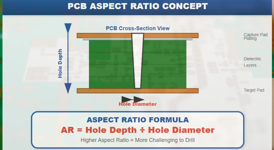
Aspect Ratio PCB Structure and Advanced Drilling Requirements
A typical high aspect ratio PCB must maintain reliable electrical connectivity through extremely deep holes relative to their diameter, often exceeding 10:1 ratios in thick multilayer designs. The core manufacturing challenges for aspect ratio PCB include:
- Precision mechanical drilling for holes as small as 0.1mm in boards up to 8mm thick
- Advanced laser drilling technology for microvias with aspect ratios up to 1:1 in HDI PCB designs
- Specialized copper plating processes ensuring uniform coverage in high aspect ratio holes
- Sequential lamination techniques for complex layer stackups requiring multiple drilling operations
- Quality control methods validating electrical connectivity through extreme aspect ratio vias
- Environmental stress testing ensuring long-term reliability under thermal cycling
High aspect ratio PCB designs typically employ sophisticated multilayer PCB stackups with layer counts from 16 to 64 layers. The challenge lies in maintaining drill quality and plating uniformity as hole depth increases relative to diameter. Advanced designs integrate laser-drilled microvias, mechanically drilled through-holes, and blind/buried via combinations to optimize routing density while managing aspect ratio constraints.
Modern communication infrastructure and computing systems require aspect ratios that challenge conventional manufacturing limits, demanding specialized equipment and process optimization.
Specialized Manufacturing for High Aspect Ratio Challenges
Our production capabilities are specifically optimized for the demanding requirements of aspect ratio PCB manufacturing across all via types and board thicknesses:
- Mechanical Drilling: Precision spindles maintaining 0.025mm drill accuracy through boards up to 8mm thick
- Laser Drilling Technology: UV and CO2 laser systems for microvias with 0.05-0.3mm diameters
- Advanced Plating Processes: Specialized chemistry and current profiles for uniform copper distribution in deep holes
- Backplane PCB Capability: Extreme thickness boards up to 12mm with aspect ratios exceeding 20:1
- Sequential Lamination: Multiple press cycles enabling complex via structures in thick multilayer designs
- Via Fill Technology: Conductive and non-conductive fill materials optimizing electrical and mechanical performance
Manufacturing processes utilize state-of-the-art drilling equipment with automatic tool wear monitoring, advanced plating bath control maintaining precise chemistry balance, and comprehensive inspection systems validating hole quality at every process step. Our turnkey assembly services include electrical testing, cross-sectional analysis, and reliability validation for high aspect ratio designs.
Drilling Technology and Process Optimization Strategies
Achieving reliable high aspect ratio PCBs requires sophisticated drilling technologies and precise process control. Effective aspect ratio management is critical—not only for maintaining electrical connectivity, but also for ensuring mechanical reliability, thermal performance, and manufacturing yield optimization.
Drilling Technology by Application Type
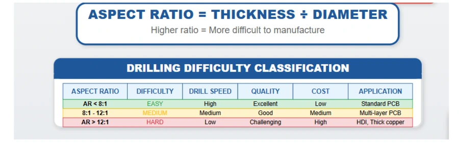
- Standard Through-Hole (5:1 to 8:1 Aspect Ratio) Focus on conventional mechanical drilling with optimized feed rates and spindle speeds for consistent hole quality and tool life management.
- High Aspect Ratio Through-Hole (8:1 to 15:1) Implements specialized drill geometries, advanced chip evacuation, and precision spindle control to maintain hole quality in thick multilayer designs.
- Extreme Aspect Ratio (15:1 to 25:1) Requires custom drill designs, sequential drilling operations, and specialized plating processes to achieve reliable electrical connectivity.
- HDI Microvia Applications (0.5:1 to 1:1) Must support laser drilling precision with controlled taper angles and optimal landing pad designs for maximum reliability.
- Mixed Technology Designs Combines mechanical and laser drilling with sequential lamination to optimize routing density while managing aspect ratio constraints.
Quality Control and Reliability Considerations
- Hole Quality Inspection Advanced optical and X-ray inspection systems validate hole geometry, including taper angles, surface roughness, and drilling debris removal.
- Plating Uniformity Validation Cross-sectional analysis and electrical testing ensure uniform copper distribution throughout high aspect ratio holes with comprehensive thickness measurements.
- Mechanical Reliability Testing Thermal cycling, mechanical stress testing, and accelerated aging validate long-term reliability of high aspect ratio via connections.
- Rigid-flex PCB Integration Specialized techniques manage aspect ratio challenges in flexible sections while maintaining electrical and mechanical integrity through bend cycles.
Aspect Ratio PCB Applications and Manufacturing Segments
Aspect ratio PCB technology serves diverse manufacturing segments, each with specific technical requirements:
- Server and Computing Systems for High-Layer-Count Motherboards and Processor Modules
- Telecommunications Infrastructure including 5G Base Stations and Network Equipment
- Automotive Electronics with Thick ECU Boards and Power Management Systems
- Aerospace and Defense requiring Ultra-Reliable High-Density Interconnects
- Industrial Control Systems with Robust Multilayer Designs for Harsh Environments
- Medical Equipment demanding High-Reliability Implantable and Diagnostic Devices
- Test and Measurement requiring Precision Signal Routing in Complex Instruments
Advanced applications increasingly require mixed aspect ratio designs combining different via technologies on single PCBs. Our specialized manufacturing enables optimal routing solutions while managing the complex interactions between different drilling and plating processes.
Integrated Manufacturing Solutions for Complex Designs
Beyond core aspect ratio PCB manufacturing, we provide comprehensive design and manufacturing support:
Advanced Design Services:
- Aspect ratio optimization analysis for maximum routing density
- Layer stackup design minimizing drilling complexity and cost
- Via technology selection balancing performance and manufacturability
- Thermal and mechanical stress analysis for high aspect ratio designs
Specialized Process Development:
- Custom drill tool design for unique aspect ratio requirements
- Plating process optimization for specific material combinations
- Sequential lamination planning for complex multilayer stackups
- Quality control procedures tailored to specific aspect ratio challenges
System Integration Support:
- Design rule development for high aspect ratio manufacturability
- Prototyping and validation services for new aspect ratio technologies
- Volume production scaling from development through high-volume manufacturing
- Failure analysis and process optimization for challenging aspect ratio designs
Why Choose HILPCB for Aspect Ratio PCB Manufacturing
The modern electronics market demands exceptional precision, reliability, and innovation in high aspect ratio PCB manufacturing. HILPCB combines advanced drilling technology with deep expertise in multilayer design and precision manufacturing to support brands delivering cutting-edge electronic products.
We are ISO 9001:2015 and IPC-A-600 Class 3 certified, with specialized capabilities in high aspect ratio manufacturing and comprehensive quality control. Our engineering teams provide drilling optimization, stackup design, and reliability analysis specifically for challenging aspect ratio applications. From prototype development to high-volume production, we ensure reliable delivery with focus on electrical performance, mechanical reliability, and manufacturing cost optimization.
Frequently Asked Questions — Aspect Ratio PCB
Q1: What is the maximum aspect ratio achievable in PCB manufacturing?
A: We can achieve aspect ratios up to 25:1 for specialized applications using advanced drilling and plating processes. Standard production typically supports up to 12:1, with aspect ratios above 15:1 requiring specialized equipment and enhanced process controls.
Q2: How does aspect ratio affect PCB manufacturing cost?
A: Higher aspect ratios increase manufacturing complexity and cost due to specialized drilling requirements, longer plating times, and additional quality control steps. Aspect ratios above 10:1 typically require premium processing with associated cost increases.
Q3: What quality control methods validate high aspect ratio via reliability?
A: We employ cross-sectional analysis, electrical continuity testing, thermal cycling validation, and advanced imaging techniques to ensure copper plating uniformity and long-term reliability in high aspect ratio vias.
Q4: Can aspect ratio limitations be overcome through design optimization?
A: Yes, design techniques including blind/buried vias, sequential lamination, and HDI technology can reduce effective aspect ratios while maintaining routing density. We provide design consulting to optimize stackups for manufacturability.
Q5: How does material selection affect aspect ratio PCB manufacturing?
A: Substrate material properties including thermal expansion, drilling characteristics, and plating adhesion affect high aspect ratio via reliability. We recommend materials optimized for your specific aspect ratio requirements and operating conditions.
Q6: What applications benefit most from high aspect ratio PCB technology?
A: High-performance computing, telecommunications infrastructure, aerospace systems, and automotive electronics benefit from high aspect ratio designs that enable maximum routing density in constrained form factors while maintaining signal integrity.