
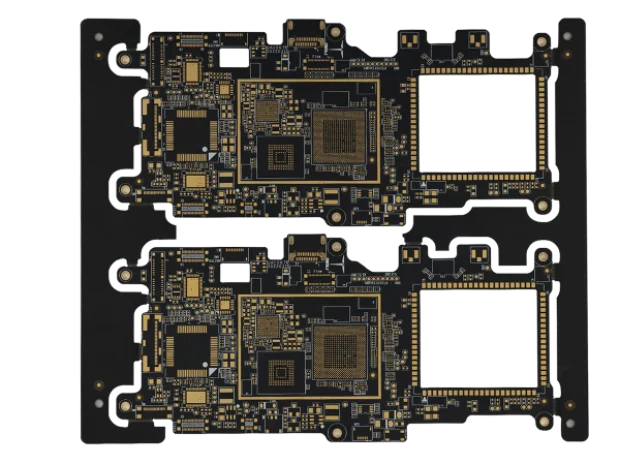
When high-speed signals transition between layers in a multi-layer printed circuit board, the unused portion of the plated through-hole (PTH) acts as a resonant antenna known as a "via stub." In 10G to 56G+ SerDes channels, this stub causes severe impedance discontinuities, signal reflections, and excess insertion loss, ultimately closing the data eye. Backdrilling (also known as controlled-depth drilling) is the manufacturing process used to physically remove this unused copper barrel from the PCB, pushing the resonance frequency out of the critical signal bandwidth.
However, backdrilling is not a simple push-button operation. It involves tight mechanical tolerances, specialized drill bits, primary and secondary drill passes, and strict antipad clearances. Specifying "just backdrill the high-speed nets" is insufficient for a production release.
This guide provides a structured approach for hardware engineers, PCB designers, and NPI teams to define, review, and release backdrilled boards to fabrication with predictable performance and zero manufacturing ambiguity.
In This Guide
- How does a via stub degrade signal integrity?
- Backdrill vs. Blind/Buried Vias: Which should you choose?
- How to specify backdrill depth and residual stub tolerances?
- What are the critical layout and DFM rules for backdrilling?
- What must be included in a backdrill PCB RFQ checklist?
- FAQ
How does a via stub degrade signal integrity?
A via stub behaves as an open-ended transmission line branching off the main signal path. Because the end of the stub is an open circuit, the signal wave traveling down the stub reflects back toward the junction. When the reflected wave arrives exactly 180 degrees out of phase with the primary signal, they cancel each other out, creating a sharp dip in the channel’s frequency response (often called a "suckout" or resonance null).
The frequency of this resonance null depends directly on the physical length of the stub:
Resonance Frequency (GHz) ≈ c / (4 * Stub Length * sqrt(Dk))
For example, a 40-mil via stub in FR4 (Dk ≈ 4.0) will create a massive resonance null around 35–40 GHz, devastating the performance of a 28 Gbps or 56 Gbps PAM4 channel. By backdrilling the via and reducing the stub to a residual 8 mils, the resonance frequency is pushed well beyond 100 GHz, leaving the operational bandwidth clean.
Backdrill vs. Blind/Buried Vias: Which should you choose?
While HDI (High-Density Interconnect) techniques like blind and buried vias also eliminate via stubs, they fundamentally change the PCB construction process. Backdrilling is performed on a standard sequential laminated board, making it often more cost-effective for thick backplanes or line cards that do not otherwise require HDI.
Decision Matrix: Via Stub Mitigation Strategies
| Mitigation Technique | Process Impact | Cost Implication | Best Use Case | Primary Limitation |
|---|---|---|---|---|
| Backdrilling (Controlled Depth) | Adds secondary drill and plating removal steps; requires antipad clearances | Moderate (adds 10-20% to bare board cost depending on drill count) | High-speed backplanes, 100G/400G switch line cards, thick boards (e.g., >100 mil) | Mechanical depth tolerance leaves a residual stub (typically 8-10 mils); consumes routing space. |
| Blind/Buried Vias (HDI) | Requires sequential lamination (multiple press cycles) | High (can double bare board cost for multiple laminations) | Dense mobile/wearable boards, complex BGA escapes, space-constrained designs | Aspect ratio limits restrict blind via depth; expensive for high layer counts. |
| Top-to-Bottom Routing | No process impact (standard PTH) | None (Standard fabrication) | High-speed links on thin boards (e.g., PCIe cards) | Constrains layout; requires all high-speed signals to transition across the entire stackup. |
| Microvias (Any-Layer HDI) | Laser drilling, copper filling, sequential buildup | Highest | Ultra-dense SoCs, smartphones, radars | Cost-prohibitive for large-format infrastructure boards. |
For a standard 12-layer to 24-layer server motherboard where high-speed routing must transition from Layer 1 to Layer 6, backdrilling from the bottom (Layer 24 up to Layer 7) is almost always the most balanced engineering decision compared to adding 4 extra lamination cycles.
How to specify backdrill depth and residual stub tolerances?
A manufacturer cannot drill perfectly to the exact micron of the signal layer. The drill bit has a conical tip, the PCB material has thickness variations (dielectric pressing tolerances), and the Z-axis drilling machine has mechanical limits.
Because of this, you must specify a Residual Stub Target rather than expecting zero stub.
- Primary PTH Drill: The initial through-hole is drilled and plated.
- Backdrill Pass: A slightly larger drill bit is used to drill down to a specific depth, removing the plating.
- Residual Stub: The remaining un-drilled portion of the via barrel below the active signal layer.
- Safety Margin (Keep-out): The dielectric space between the tip of the backdrill and the active signal layer to prevent accidentally severing the trace.
Industry Standard Tolerances:
- Standard Backdrill: Residual stub of 8 to 12 mils (0.20 mm – 0.30 mm).
- Precision Backdrill: Residual stub of 6 to 8 mils (0.15 mm – 0.20 mm). (Requires advanced depth-mapping equipment).
When defining the stackup, ensure that the dielectric thickness between the signal layer and the layer where the backdrill stops is thick enough to accommodate the drill depth tolerance (usually at least 4-5 mils).
What are the critical layout and DFM rules for backdrilling?
Providing incomplete CAD data is the leading cause of backdrill manufacturing delays. A backdrilled hole is physically larger than the original via, which means copper clearances must be expanded. Review these rules before tape-out:
1. Backdrill Diameter and Antipad Sizing
The backdrill bit is typically 6 to 10 mils (0.15–0.25 mm) larger than the primary via drill size. If your primary via is 10 mils, the backdrill will be 18 mils.
- Rule: The antipad (copper clearance) on all layers penetrated by the backdrill must be sized to clear the backdrill diameter plus a registration tolerance (e.g., Backdrill Diameter + 10 mils).
- Risk: Failure to enlarge antipads will result in the backdrill barrel shorting to inner ground or power planes.
2. Identify Backdrill Sides
Backdrilling can be done from the Top side, Bottom side, or both.
- Rule: Clearly identify the "From-To" layers for every backdrill group in your fabrication drawing (e.g., "Backdrill from Bottom Layer to Layer 5").
3. Trace Keep-Out Zones
- Rule: Do not route traces on adjacent layers near the backdrill target zone. The conical tip of the drill could penetrate slightly deeper than expected.
- Rule: The active signal trace (the one you are trying to preserve) must exit the via strictly within the remaining plated barrel zone.
4. Non-Functional Pads (NFP)
- Rule: Remove non-functional pads on all layers that the backdrill passes through. Leaving them in place can cause drill bit wander and excessive wear.
What must be included in a backdrill PCB RFQ checklist?
To ensure the PCB manufacturer quotes the exact electrical performance and construction you need, your Request for Quote (RFQ) must move beyond generic Gerber files. Include the following explicit backdrill specifications:
Design Package Requirements
- NC Drill Files: Must include separate, explicit drill files for the backdrill passes (do not merge them with standard PTH files).
- Fabrication Drawing: A clearly defined backdrill table listing:
- Drill file name
- Drill size (primary and backdrill)
- Start layer and End layer (e.g., Bottom to L8)
- Must Not Cut layer (e.g., L7)
- Max allowed residual stub length (e.g., < 10 mils)
- Stackup Drawing: Showing nominal dielectric thicknesses and identifying the backdrill depth stops.
Validation and Evidence Request
- Impedance/TDR Report: Specify if TDR testing is required on backdrilled coupon structures.
- Cross-Section (Microsection) Report: Mandate a cross-section report of a backdrilled via to visually verify the residual stub length and confirm no damage occurred to the active signal layer connection.
- Electrical Test (Netlist): Confirm 100% bare board electrical test after the backdrill process is completed to verify no open circuits (severed traces) or shorts.
FAQ
What problem does backdrill solve in high-speed PCB design?
Backdrill removes unused via stub length below the last connected layer, which reduces resonant behavior, reflections, and excess loss on high-speed channels. In SerDes and other fast links, this helps improve eye opening, return loss, and overall signal integrity margin.
When does a PCB design usually need backdrill?
Backdrill is typically considered when data rates rise above 10 Gbps, layer transitions become unavoidable, and via stubs start consuming too much of the channel budget. It is especially common in backplanes, networking hardware, AI servers, and thick boards where long vias materially hurt link performance.
Can backdrilling be done from both sides of the PCB?
Yes, a single via can be backdrilled from both the Top and Bottom sides simultaneously. For example, a signal transitioning from Layer 4 to Layer 6 on a 20-layer board could have the stub removed from the Top (L1 down to L3) and from the Bottom (L20 up to L7).
What residual stub target is common after backdrill?
Many projects target a residual stub below 8 to 10 mils, but the correct value depends on frequency content, stackup, and channel budget. The target should be set from signal integrity simulations rather than copied as a fixed rule across every design.
What manufacturing controls matter most for a successful backdrill PCB?
Successful backdrill work depends on drill registration, depth control, stackup definition, copper clearance (antipads), and clear fabrication notes that identify the affected nets. Designers and fabricators also need aligned inspection methods (like cross-sectioning) so the electrical benefit is confirmed.
Next steps
HILPCB can review your high-speed layout, evaluate stackup feasibility, and quote your backdrill requirements with precision. We ensure that DFM checks for antipads, stub tolerances, and drill registration are fully aligned with your signal integrity goals before fabrication begins.
Use the full Request a Quote form and include your Gerber/ODB++ files, stackup requirements, and backdrill table. Our engineering team will review the design for manufacturability and outline the exact inspection evidence (like cross-section reports for residual stub verification) included in your order.