HilPCB Engineering Services

PCB Design & Layout Services

Factory-integrated printed circuit board design services connecting schematic capture and constraint-driven layout directly to bare-board fabrication and turnkey SMT assembly. Our PCB designers build your stackup around real stocked laminates, verify IPC-7351 footprints against active MPNs, and hand over 100% unlocked native CAD databases.

Factory-integrated PCB design and layout services
1โ€“32+L
Rigid, Flex, Rigid-Flex & HDI Layout
100%
Unlocked Native CAD IP Ownership
IPC-7351
Verified Land Patterns & DFM Rules
Turnkey
Direct Handoff to Fab & SMT Lines
  • IPC-2221 / IPC-7351Constraint & Footprint Standards
  • IPC-6012 Class 2/3Fab-Aligned Design Rules
  • ODB++ & IPC-2581Intelligent CAM Handoff
  • AVL BOM ScrubLive Lifecycle & Stock Check

01 ยท HilPCB Engineering Services

PCB Design Capability Matrix

โšก
Engagement scopes
Full schematic + layout, netlist-to-Gerber layout, EOL/EMC board redesign, or pre-fab DFM/DFA audit
๐Ÿ“
Supported ECAD tools
Altium Designer, Cadence Allegro / OrCAD, PADS, and KiCad with 100% unlocked native source handoff
๐Ÿงช
Layer & HDI capability
1 to 32+ layers, Type Iโ€“III HDI, blind/buried microvias, VIPPO, 0.35โ€“0.4 mm pitch BGA escape
๐Ÿ“ฆ
High-speed & RF design
DDR4/DDR5, PCIe Gen 4/5, USB4, 10Gโ€“100G SerDes, sub-6 GHz RF, and hybrid Rogers/Megtron stackups
๐Ÿ›ก๏ธ
Manufacturing integration
Stackup and material availability reviewed with the factory; BOM lifecycle, sourcing, and approved substitutions reviewed before procurement
๐Ÿงฐ
Complete deliverables
Native CAD, ODB++ / IPC-2581, Gerber X2, NC Drill, Master Fab Drawing, XYR Centroid, 3D STEP, and AVL BOM

02 ยท Representative PCB Design & Layout Scenarios

Representative PCB Design & Layout Scenarios

Three common ways hardware teams use our PCB design and layout services to accelerate NPI schedules and reduce avoidable fabrication respins.

Engineering Example

High-Speed Multilayer SOM & Carrier Board Layout

10-to-16 layer HDI layout featuring 0.4 mm pitch BGA escape via VIPPO, DDR4/DDR5 fly-by length tuning, and PCIe Gen 4 differential pairs modeled on low-loss laminate stock before routing.

Read controlled-impedance stackup rules
Engineering Example

Industrial Motor Drive & BMS Heavy-Copper Layout

4-to-6 layer mixed-signal power layout separating high-dV/dt gate-drive loops from precision current-sense amplifiers, with IPC-2152 polygon sizing and thermal via arrays.

Explore heavy-copper PCB capabilities
Engineering Example

EOL Component Redesign & Turnkey PCBA Migration

Rapid schematic and footprint migration replacing discontinued microcontrollers and LDOs with active second-source alternatives while preserving the existing enclosure mounting footprint.

See turnkey PCB assembly workflow

03 ยท Which PCB Design Service Scope Fits Your Project?

Which PCB Design Service Scope Fits Your Project?

  • 01Full Concept-to-Layout (Circuit Design Services + Layout): Ideal for teams starting from a system block diagram or functional spec. Includes architecture review, schematic capture, active MPN selection, and complete PCB layout.
  • 02Netlist-to-Gerber (PCB Design and Layout Services): Ideal for hardware teams with a verified schematic in Altium, OrCAD, or KiCad who need an experienced PCB layout designer to handle stackup modeling, 3D placement, and high-speed constraint routing.
  • 03Legacy Board Respin & EOL Redesign: Replace obsolete/NRND semiconductors, resolve EMC/thermal failures, or migrate a through-hole board to compact surface-mount technology without breaking enclosure compatibility.
  • 04Pre-Fabrication DFM, Stackup & Library Audit: Have our CAM and SMT engineers validate your in-house designer PCB database against live laminate stock, IPC-7351 pad rules, and stencil aperture ratios before tooling release.

04 ยท What Our PCB Layout & Engineering Team Delivers

What Our PCB Layout & Engineering Team Delivers

Our PCB design team coordinates schematic capture, layout, simulation, and component selection with the CAM and assembly engineers responsible for the manufacturing route. Agree etching, lamination, footprint, and SMT constraints before routing so the released design can move into fabrication and assembly with a documented baseline.

  • Real-stock stackup and 2D field-solver impedance modeling (50 ฮฉ single-ended, 85 ฮฉ PCIe, 90 ฮฉ USB, 100 ฮฉ differential Ethernet where specified; DDR targets set from the controller and memory guidance) matched to stocked FR-4, High-Tg, Rogers, and Megtron laminates.
  • High-density interconnect (HDI) escape routing for 0.35โ€“0.50 mm pitch BGAs/QFNs using staggered or stacked laser microvias and Via-in-Pad Plated Over (VIPPO).
  • Power electronics and high-voltage layout per IPC-2152 current-capacity curves and UL/IEC creepage/clearance isolation rules on 2 oz to 10 oz copper.
  • 3D ECAD-MCAD collision verification using STEP enclosure models to lock connector protrusions, mounting holes, thermal sinks, and rigid-flex bend radii.
  • BOM lifecycle and availability review during schematic and footprint assignment: confirm the exact manufacturer part number, package and ordering suffix, approved sources, and customer-approved alternates before procurement.
  • Full unlocked IP handoff: native CAD schematic and layout files, ODB++ / IPC-2581, Gerber X2, NC Drill, Master Fab Drawing, XYR Centroid, and scrubbed Excel BOM.
  • Clear change and validation boundaries: a component substitution is not automatically a drop-in replacement, DRC checks configured rules while DFM checks the intended manufacturing route, and neither replaces product-level functional or compliance testing.
  • Input quality decides the outcome: the PCB board designer cannot set meaningful routing rules from interface names alone, so our circuit board design & layout services start from your netlist, mechanical constraints, and target impedance table.

05 ยท Design-to-Manufacturing Workflow & Sign-Off Gates

Design-to-Manufacturing Workflow & Sign-Off Gates

Every circuit board design service project runs through four customer sign-off gates so stackup, placement, routing, and BOM procurement stay synchronized before fabrication begins.

  1. ๐Ÿ“ค1

    Submit Design Inputs

    Submit your schematic (or block diagram), preliminary BOM, 2D/3D mechanical outline (DXF/STEP), and target electrical/environmental constraints.

  2. ๐Ÿ”2

    Gate 1 โ€” Stackup & Library Lock

    Gate 1 โ€” Stackup & Library Lock: Our engineers verify schematic ERC rules, scrub MPN lifecycle status, and propose a factory-verified layer stackup and impedance table.

  3. ๐Ÿ“‹3

    Gate 2 โ€” Placement Approval

    Gate 2 โ€” 3D Placement Approval: We place all critical connectors, high-speed ICs, and thermal components and send a 3D STEP/PDF check plot for your sign-off before routing.

  4. ๐Ÿญ4

    Gate 3 โ€” Routing & DFM Audit

    Gate 3 โ€” Constraint Routing & CAM DFM Audit: Traces are routed with length/skew matching and solid return paths, then audited directly in factory CAM and SMT DFA software.

  5. ๐Ÿ“ฆ5

    Gate 4 โ€” File Delivery & Build Handoff

    Gate 4 โ€” Unlocked File Delivery & Turnkey Build: Receive 100% unlocked native CAD and manufacturing files, or transition directly into bare-board fabrication and turnkey PCBA.

06 ยท PCB Design RFQ Checklist

PCB Design RFQ Checklist

For PCB design services outsourcing with impedance control, include the target nets, stackup constraints, impedance requirements and tolerances, and the intended fabricator. For other projects, send the applicable items below so our PCB design engineer can return a fixed-price or milestone quotation with a proposed stackup and schedule.

RequiredSchematic or Block Diagram
Native Altium, OrCAD, or KiCad schematic (or searchable PDF with netlist). Required to count pins, nets, and power rails for quoting.
Use TBD when unsure. Our PCB designers confirm stackup and constraints before quoting.

RequiredPreliminary Bill of Materials (BOM)
Excel or CSV list of key ICs, connectors, and critical passives with MPNs. Needed to verify package footprints and stock availability.
Use TBD when unsure. Our PCB designers confirm stackup and constraints before quoting.
RequiredMechanical Outline & Keep-Outs (DXF / STEP)
Board contour, mounting hole locations, fixed connector coordinates, and component height limits.
Use TBD when unsure. Our PCB designers confirm stackup and constraints before quoting.
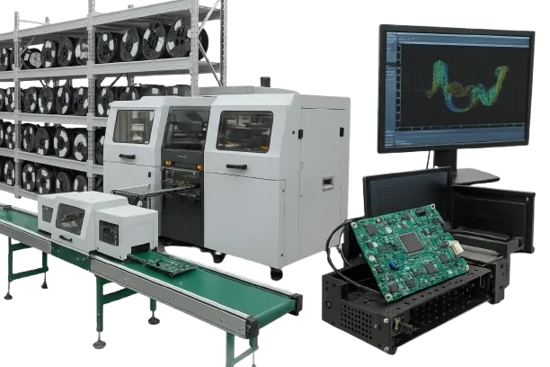
RequiredHigh-Speed & Impedance Constraints
Target layer count, controlled-impedance buses (DDR, PCIe, Ethernet, RF), maximum trace lengths, and differential skew budgets.
Use TBD when unsure. Our PCB designers confirm stackup and constraints before quoting.
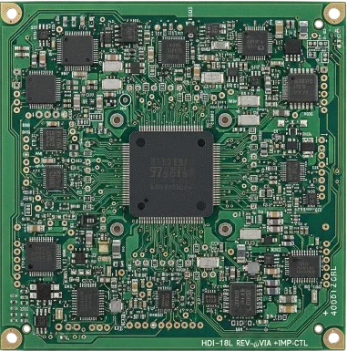
RequiredPower, Thermal & Isolation Specs
Rail currents, maximum ambient temperature, heavy-copper requirements, and high-voltage creepage/clearance targets.
Use TBD when unsure. Our PCB designers confirm stackup and constraints before quoting.
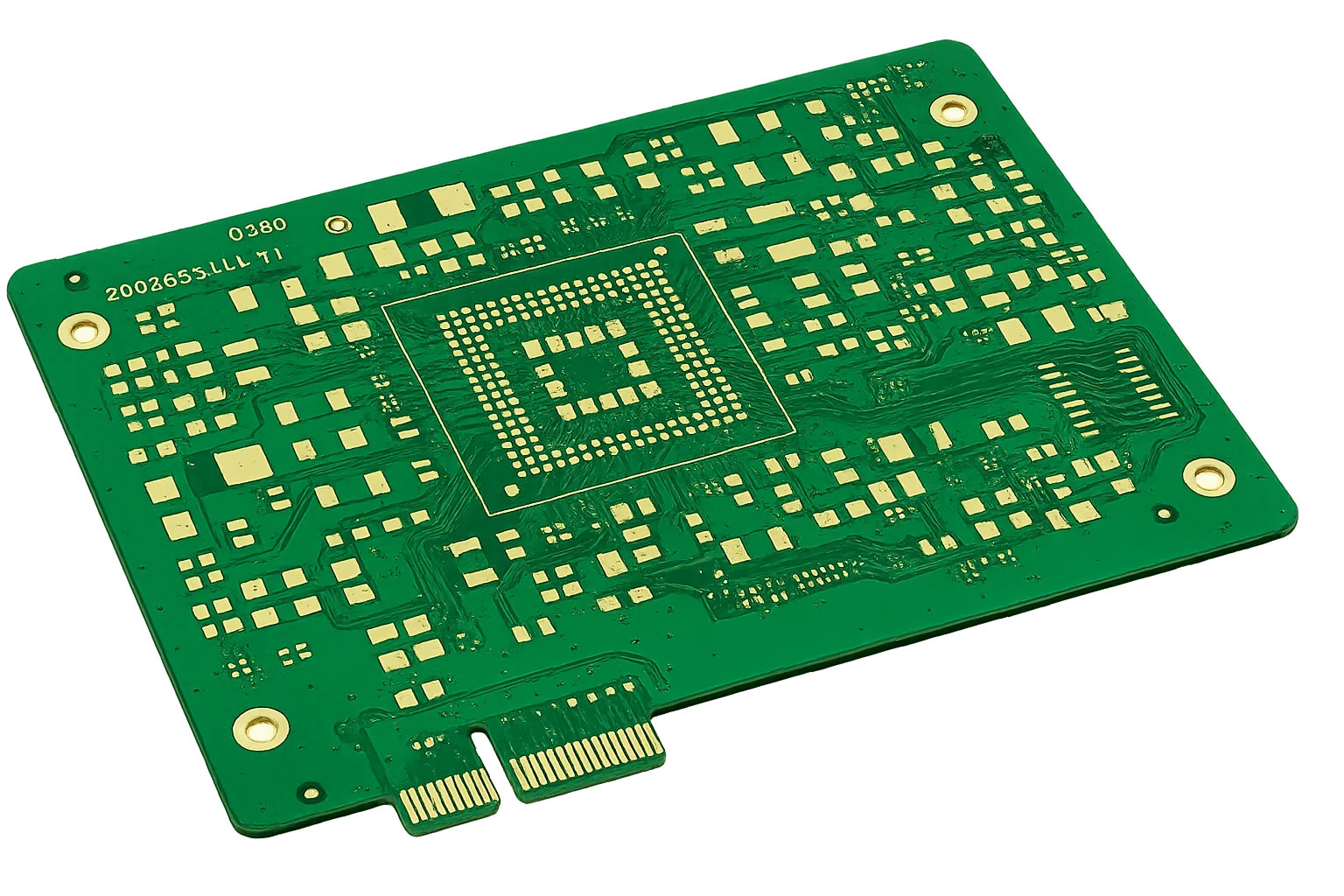
RequiredTarget Deliverable & Build Scope
Preferred native ECAD format, IPC Class 2 or Class 3 workmanship target, and prototype quantity if bundling turnkey assembly.
Use TBD when unsure. Our PCB designers confirm stackup and constraints before quoting.
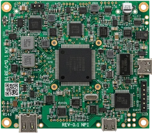
07 ยท Frequently Asked Questions on PCB Design Services

Frequently Asked Questions on PCB Design Services

Which ECAD software platforms do your PCB designers support?

Our circuit board designers work natively in Altium Designer, Cadence Allegro / OrCAD, PADS, and KiCad. Upon completion, we hand over the unlocked native schematic and PCB layout databases alongside ODB++, IPC-2581, Gerber X2, Excellon drill, 3D STEP, and pick-and-place centroid (XYR) files.

Do I retain 100% ownership of the native PCB design files?

Yes. You retain full intellectual property (IP) and file ownership of all schematics, custom component libraries, and layout databases created during the project. All deliverables are provided unlocked with no vendor lock-in.

How is PCB design cost calculated?

PCB design cost is quoted as a fixed project fee or milestone package based on total pin count, net count, layer count, high-speed length/impedance constraints, and mechanical complexity. Share your schematic and board outline with our team to receive a scoped engineering quote and schedule.

Why choose a manufacturer's PCB design service over a standalone layout bureau?

Factory-integrated PCB design coordinates the layout with the intended stackup, material availability, via process, footprint, and assembly constraints before release. Our PCB layout engineers work with CAM and SMT teams so the quotation and design review can define the applicable rules and evidence. Compare providers by their review records, agreed deliverables, and change-control process.

Can you start from a hand-drawn schematic or system block diagram?

Yes. Under our full circuit design services scope, our hardware engineers can capture the formal schematic, select active components with approved second-source alternates, run Electrical Rules Checks (ERC), and proceed into PCB layout after your schematic sign-off.

Can I bundle PCB design services with prototype fabrication and SMT assembly?

Yes. Combining our PCB design and assembly services lets your project move straight from layout sign-off into bare-board fabrication, authorized BOM procurement, and automated SMT assembly under a single project timeline and engineering contact.

Ready to Start Your PCB Design or Layout Project?

Upload your schematic, block diagram, or legacy filesโ€”our engineering team will review your constraints and return a scoped quotation.