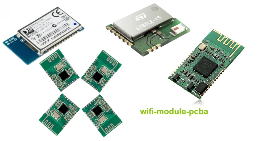
At Highleap PCB Factory, we design and manufacture wireless electronics for all short-range communication applications—extending far beyond Bluetooth modules. From industrial IoT sensors and medical device telemetry to automotive connectivity and wearable electronics, our expertise in low-power wireless PCB design ensures optimal performance across all industries. While this guide focuses on Bluetooth PCB design solutions, our comprehensive manufacturing capabilities span every electronic application. Whether you need flex PCB for wearables or HDI PCB for ultra-compact devices, Highleap PCB Factory delivers complete PCB manufacturing and assembly services for innovative wireless solutions across all sectors.
Bluetooth Low Energy (BLE) Optimization
Modern Bluetooth PCB designs emphasize ultra-low power consumption for years-long battery life and reliable smart home or IoT connectivity.
Bluetooth 5.0+ offers up to 4x greater range, 8x higher data capacity, and lower power use, supporting whole-home coverage and advanced, high-data applications.
Ultra-Low Power Design: Power management and optimized sleep modes let devices run for months or years on a single battery, with instant wake times and efficient data transmission.
Mesh Networking: Bluetooth mesh supports large, self-healing device networks. Our multilayer PCB designs ensure robust mesh implementation for scalable automation.
Multi-Protocol Coexistence: Careful RF design allows stable Bluetooth, WiFi, and Zigbee operation without interference.
Smart lock PCB solutions leverage BLE’s security and efficiency, while WiFi module PCB integration bridges Bluetooth devices with cloud connectivity for complete smart home systems.
Advanced Audio Codecs and Low-Latency Performance
Modern Bluetooth audio applications demand high-quality codecs and minimal latency transmission for superior user experience in entertainment and communication applications.
High-Resolution Audio Support: Advanced audio codecs including aptX, aptX HD, LDAC, and emerging LC3 enable CD-quality wireless audio transmission with minimal compression artifacts. Adaptive bitrate algorithms optimize audio quality based on connection conditions while maintaining consistent performance.
Low-Latency Gaming Audio: Gaming and interactive applications require sub-40ms audio latency for responsive feedback. Dedicated low-latency modes optimize transmission scheduling and buffer management while hardware acceleration reduces processing delays throughout the audio pipeline.
Multi-Device Audio Sharing: Advanced audio sharing capabilities enable multiple headphones connecting to single sources while broadcast audio features support assistive listening applications. Synchronization algorithms ensure coordinated audio playback across multiple devices.
Smart speaker PCB designs benefit from advanced Bluetooth audio features enabling high-quality wireless music streaming from smartphones and tablets. Multiple codec support ensures compatibility with various source devices while maintaining optimal audio quality.
Voice Processing Integration: Voice control PCB features enable hands-free operation through Bluetooth-connected devices. Advanced noise cancellation and echo suppression algorithms ensure clear voice communication despite challenging acoustic environments.
Optimized Bluetooth PCB Design for Reliable Wireless and Smart Home Applications
Bluetooth PCB solutions demand a holistic approach to hardware engineering—where antenna design, RF optimization, robust security, and precise manufacturing converge to deliver reliable performance across diverse environments and use cases.
Integrated PCB Antenna Engineering: Leveraging advanced antenna structures—such as inverted-F, monopole, and meandered traces—directly on the PCB, we achieve compact integration without sacrificing signal quality. These designs are further enhanced through diversity systems and adaptive tuning, allowing Bluetooth modules to maintain strong connections even in crowded or variable RF environments. Spatial and pattern diversity, along with automatic antenna switching, ensure stable communication for both smart home and industrial deployments.
RF Coexistence and Environmental Adaptability: Our PCB layouts and stack-ups are engineered to mitigate interference between Bluetooth, WiFi, and other radios, employing isolation, filtering, and careful component placement. Adaptive tuning systems and robust PCB material selection compensate for proximity effects, enclosure variances, and the presence of human users, ensuring consistent wireless performance.
Security by Design: Protecting user data and device integrity is paramount. Our Bluetooth PCBs implement AES-128 encryption, secure pairing protocols, privacy features such as random address generation, and OTA security updates. For applications like security camera PCB and smart doorbell PCB, we incorporate end-to-end encryption and secure boot processes, providing uncompromising protection for sensitive data and video streams.
Manufacturing Precision and Quality Assurance: Bluetooth modules require high-density PCB integration, often realized through HDI PCB techniques—using microvias, blind/buried vias, and fine-pitch components to achieve compact, high-performance layouts. Rigorous RF validation, automated functional testing, and comprehensive environmental qualification (including vibration, temperature, and humidity cycling) guarantee product reliability. Our turnkey assembly solutions encompass sourcing, assembly, and full traceability for each build.
Seamless Smart Home and Ecosystem Integration: Bluetooth PCBs power modern smart home devices with compatibility for platforms like Apple HomeKit, Google Assistant, Alexa, and SmartThings. Our designs support home automation PCB coordination, secure device provisioning, and interoperability with Matter/Thread standards, ensuring future-proof, cross-platform connectivity. Local edge computing capabilities enhance privacy, responsiveness, and automation flexibility.
Through every phase—from antenna layout to final assembly—our Bluetooth PCB design and manufacturing expertise delivers secure, high-performance, and interoperable wireless solutions for smart devices, IoT, and advanced home automation. Trust Highleap PCB Factory to engineer the foundation of your next-generation wireless products.
Your Complete Short-Range Wireless Partner
While Bluetooth PCB designs demonstrate our wireless expertise, Highleap PCB Factory manufactures circuit boards for every short-range communication application. Industrial sensors, medical devices, automotive systems, wearable electronics—our experience with low-power wireless technologies benefits all customers requiring reliable wireless solutions. This comprehensive background ensures your Bluetooth products achieve exceptional performance and battery life.
From IoT prototypes to high-volume consumer devices, our integrated capabilities cover every stage of production. Whether you need advanced smart-home PCB solutions for automation systems or ultra-compact modules for wearables, we deliver precision-engineered boards that meet modern wireless demands.
From initial RF design through regulatory approval to volume manufacturing, we provide complete support ensuring your Bluetooth products succeed in competitive markets. Choose Highleap PCB Factory for wireless electronics that connect efficiently and reliably.