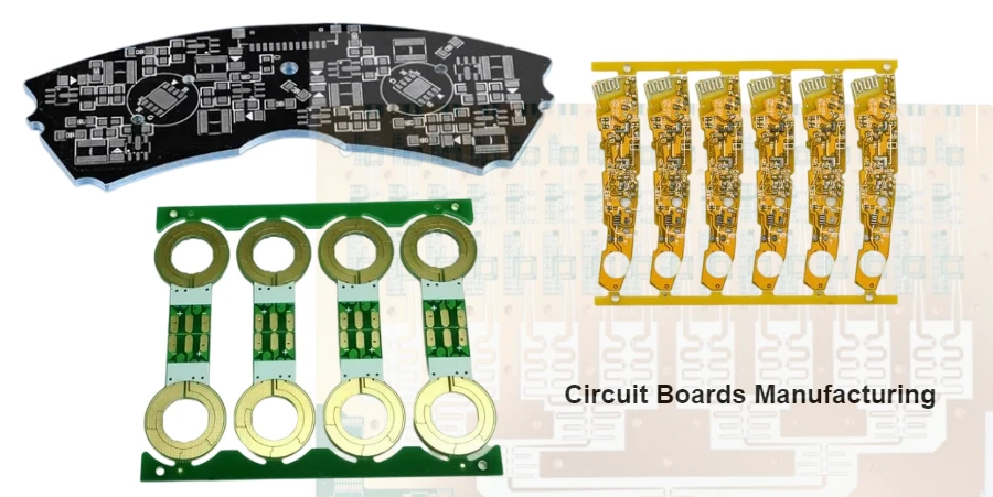
Why PCB Manufacturing Quality and Speed Matter
In today’s electronics market, choosing the right partner for circuit board manufacturing is not just about producing PCBs — it’s about ensuring reliability and protecting your brand. Poor-quality boards can cause failures, recalls, and costly delays. With precise process control, high-grade materials, and comprehensive testing, your products perform consistently and meet industry standards.
Speed is just as critical. Whether you need a quick-turn prototype or high-volume production, fast lead times help you launch products faster, capture market opportunities, and stay ahead of competitors. The ability to scale smoothly from design to mass production — including custom circuit board design and circuit board assembly — makes a real difference in time-to-market.
At Highleap PCB Factory, we combine advanced automation, ISO/IPC-certified processes, and strict quality systems to deliver both speed and precision. Our approach ensures every order, from standard boards to complex multilayer circuit boards, is manufactured to meet the highest performance standards, while giving you confidence in cost efficiency and global delivery.
Core Manufacturing Stages
Substrate Preparation
Material cutting, cleaning, and surface preparation for optimal adhesion and quality.
Layer Construction
Copper cladding, imaging, and etching to create multilayer board constructions.
Drilling Operations
Precision mechanical and laser drilling for vias and component holes.
Surface Finishing
Plating, solder mask application, and final protective coatings.
The first step in PCB manufacturing is selecting the substrate material, which forms the foundation for all other processes. The choice of material influences electrical performance, mechanical strength, and manufacturing complexity. FR4 is the most commonly used material due to its cost-effectiveness and excellent insulation properties.
For more advanced applications, materials like high-frequency laminates for RF applications, flexible polyimide films for bendable circuits, and metal-core substrates for thermal management are often used.
Material Properties and Selection Criteria
- Dielectric Constant: Impacts signal propagation and performance in high-speed applications.
- Thermal Properties: These include glass transition temperature, which determines heat resistance during processing and operation.
- Mechanical Properties: Flexural strength and dimensional stability ensure the PCB can withstand physical stresses, such as vibration and shock.
Choosing the right substrate material optimizes both performance and manufacturing efficiency, affecting the overall cost and reliability of the final product.
Circuit Board Manufacturing Process
Producing high-quality PCBs requires strict process control, advanced technology, and the ability to handle both standard and specialized requirements. Below is the integrated workflow used in professional PCB factories like Highleap PCB Factory, enhanced with advanced techniques for complex projects.
Stage 1: Core Preparation & Inner Layers
- Material cutting and controlled baking for dimensional stability
- LDI (Laser Direct Imaging) for precise registration and circuit definition
- Inner layer dry film coating, exposure, etching, and stripping
- AOI (Automated Optical Inspection) for defect detection on inner layers
- Brown oxidation treatment to strengthen lamination bonding
Stage 2: Lamination & Drilling
- Layer stackup with prepreg and copper foils pressed under heat and pressure
- Aluminum entry drilling for accurate through-holes
- Laser drilling for HDI blind and buried vias
- Deburring and desmear cleaning for proper hole wall preparation
- Electroless copper deposition and electrolytic plating for PTH formation
Stage 3: Outer Layers & Special Processing
- Outer layer imaging, copper plating, and etching for final circuits
- AOI verification to detect shorts, opens, or misalignment
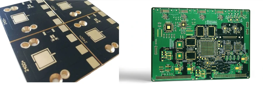
- Back-drilling to eliminate unused via stubs and improve signal integrity
- Edge plating for RF grounding and mechanical reinforcement
- Castellated holes (half holes) for module-to-board soldering
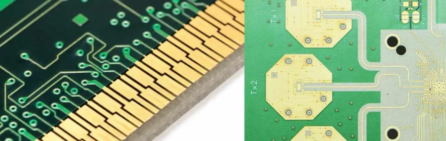
- Gold fingers plating for durable connector interfaces
- Rigid-flex integration where required for compact or foldable assemblies
Stage 4: Protection & Finishing
- Solder mask application (including via plugging for reliability)
- Silkscreen printing for reference designators and assembly guides
- Multiple finishing options: ENIG, HASL, OSP, Immersion Silver, Hard Gold
- Selective surface finishes for fine-pitch BGAs, RF designs, and aerospace boards
Stage 5: Testing & Finalization
- Impedance testing for high-speed and RF multilayer boards
- Electrical testing (continuity, isolation, high-voltage)
- Functional testing under real operating conditions
- Final inspection for cosmetic and dimensional accuracy
- Vacuum packaging and moisture-proof storage before shipping
If you need to understand the conventional multilayer PCB manufacturing workflow, you can review our detailed Multilayer Circuit Board Guide. For tailored advice on your project, our engineering team is always available—simply contact us to discuss your requirements.
China’s Most Cost-Effective Circuit Board Manufacturing
China has become the global hub for circuit board manufacturing, not only because of its scale but also due to its unmatched balance between quality, speed, and cost. Professional factories combine advanced equipment, experienced engineering teams, and strict quality systems while keeping production costs highly competitive.
At Highleap PCB Factory, we specialize in delivering high-performance, cost-effective PCBs that meet international standards. With over 15 years of manufacturing expertise, we provide solutions that range from single-layer PCBs to complex multilayer, HDI, rigid-flex, and special-process boards such as blind/buried vias, gold fingers, back-drilling, and castellated holes. This ensures our customers get the latest technology at globally competitive prices.
For international clients, our value goes beyond manufacturing. We offer one-stop PCB services, including custom circuit board design, PCB assembly, testing, and global shipping, ensuring faster project cycles and reduced total cost of ownership. By choosing Highleap, you benefit from China’s most cost-effective PCB solutions without compromising on quality or reliability.
Future Manufacturing Technologies in PCB Production
As the PCB industry evolves, new technologies such as additive manufacturing, embedded components, and Industry 4.0 technologies are helping to meet the demands for miniaturization, performance, and cost efficiency. These innovations allow for faster production, improved design flexibility, and reduced costs.
By embracing these advanced technologies, Highleap PCB Factory ensures that your circuit boards are not only of the highest quality but also produced with the latest in manufacturing capabilities. These advancements also play a critical role in the buying circuit boards process, helping customers choose the best solutions for their needs.