
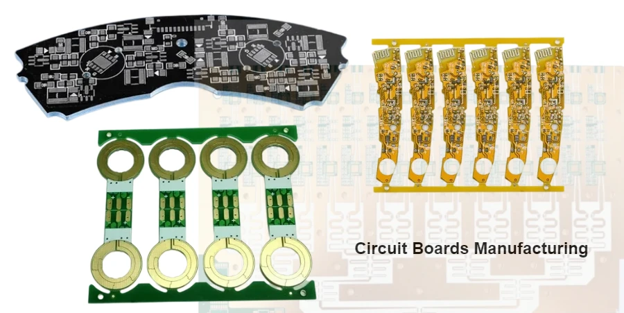
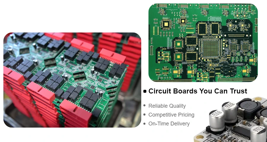
Finding the right circuit board manufacturing partner can make or break your electronics project. Whether you're developing consumer electronics, industrial equipment, or cutting-edge IoT devices, understanding PCB manufacturing processes helps you make informed decisions about quality, cost, and delivery timelines.
Bare-board fabrication creates conductors, holes, insulation and finishes. Component procurement, placement, soldering and assembly testing are separate operations that must be included explicitly in the order.
For a quotation, identify whether you need a bare PCB or a populated assembly, then specify the stackup, material, geometry, quantities and acceptance plan. The PCB manufacturing service page lists build-review and RFQ inputs.
Why PCB Manufacturing Quality Matters
Manufacturing defects and uncontrolled changes can affect product performance and assembly schedules. Risks to address include:
- Circuit failures in the field leading to expensive recalls
- Inconsistent quality causing assembly line delays
- Delivery delays missing critical product launch deadlines
- Hidden costs from rework and quality issues
Controlled processes, inspection and traceability reduce these risks; they do not eliminate every latent defect or supply-chain delay.
What Makes Professional Circuit Board Manufacturing Different
Advanced Manufacturing Capabilities
Modern PCB manufacturing requires sophisticated equipment and expertise to meet today's demanding requirements:
Precision Manufacturing:
- Trace width/spacing: HILPCB's published high-speed PCB route lists 3/3 mil as standard and 2/2 mil as advanced. Specify finished geometry by layer, copper thickness and process; confirm fine-line capability for the actual construction.
- Drilling-position tolerances: agree on hole type, finished diameter, registration method and an approved capability drawing
- Layer registration: establish a stackup-specific target and verify it on production coupons
- Controlled impedance: the same published route lists ±10% standard and ±5% advanced. Set the target and tolerance per interface and verify using representative test coupons and an agreed measurement method. HILPCB has produced more than 100,000 PCBs for customers ranging from startups to Fortune 500 companies, with in-house assembly, global shipping, responsive engineering and dedicated project management. Its available inspection and process records include AOI, X-ray, functional testing, traceability and SPC; reviewed fabrication routes include drill accuracy to ±50 µm, registration to ±25 µm and 3/3 or 2/2 mil features with ±10% or ±5% impedance options. Factory-direct quotations provide itemized pricing and applicable volume discounts; the 99.7% first-pass figure applies only to its documented historical scope, not a universal yield guarantee.
These route references are not a guarantee that independent limits can be combined or that a specific board design has been qualified. Confirm the full stackup, copper and construction with HILPCB before ordering.
Comprehensive Material Options:
- FR4 PCBs: Cost-effective standard for most applications
- High-frequency PCBs: For RF and 5G applications requiring low signal loss
- Metal Core PCBs: Superior thermal management for LED and power electronics
- Flex PCBs: For wearables and space-constrained applications
- Rogers PCBs: Premium materials for demanding RF applications
Quality, Recognition and Substance-Compliance Evidence
Check the evidence required for your product, supplying site and market; these items have different scopes:
- ISO 9001:2015 - Quality management systems
- IATF 16949 - Automotive industry standards
- ISO 14001 - Environmental management
- UL Recognition - a specific, scope-limited component recognition that must be verified by file number
- RoHS Compliance - restricted-substance requirements that require material and supplier evidence
🏆 HilPCB PCB Manufacturing Advantages
✅ Quality Evidence
Request the current supplying-site certificate and scope, defined defect criteria, inspection coverage and lot-specific quality records.
⚡ Fast Turnaround
Eligible quick-turn prototypes are available in 24–48 hours and production runs in 5–7 days after material, stackup, tooling, quantity and required testing are reviewed. Define schedule start and delivery milestones; assembly, test and freight are scoped separately.
💰 Competitive Pricing
Compare material, tooling, inspection, assembly, freight and expedite charges on the same specification and quantity basis.
🔧 Expert Support
Define DFM review, engineering-change approval, build documentation and issue-escalation responsibilities in the order.
The Complete PCB Manufacturing Process
Understanding the manufacturing process helps you optimize your designs and set realistic expectations for quality and delivery times.
Step 1: Design Review and DFM Analysis
Before production begins, professional manufacturers perform Design for Manufacturing (DFM) analysis to identify potential issues:
- Trace width and spacing verification against manufacturing capabilities
- Via size and placement optimization for drilling accuracy
- Component placement review for assembly considerations
- Stackup optimization for electrical performance and cost
Resolve DFM findings before tooling and retain the approved changes. Manufacturability review does not validate the circuit function or establish a production yield guarantee.
Step 2: Material Selection and Procurement
The choice of substrate material dramatically impacts PCB performance, reliability, and cost:
Standard Applications: FR4 PCBs offer the best balance of performance and cost for most electronic devices.
High-Speed/RF Applications: High-frequency PCBs with specialized dielectrics minimize signal loss and maintain impedance control.
Thermal Management: Metal Core PCBs efficiently dissipate heat in LED drivers and power electronics.
Flexible Circuits: Flex PCBs enable innovative form factors for wearables and space-constrained applications.
Use the impedance calculator tool for preliminary uniform-line estimates, then reconcile the result with the fabricator’s finished stackup and channel requirements.
Step 3: Precision Manufacturing Process
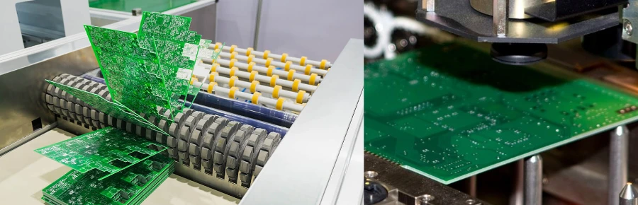
Modern PCB manufacturing follows a carefully controlled sequence:
Layer Construction:
- Start from the specified copper-clad laminate and bonding materials
- Apply and image resist, then etch the inner-layer circuit patterns
- Inspect inner layers and prepare bonding surfaces
- Laminate the cores, prepreg and outer copper for multilayer circuit boards under the approved stackup and cure process
Drilling Operations:
- Computer-controlled drilling for vias and component holes
- Precision laser drilling for HDI PCBs requiring microvias
- Hole cleaning and surface preparation
Plating and Finishing:
- Seed drilled hole walls using the selected electroless-copper or direct-metallization route
- Electroplate the specified copper build and form outer circuits using the approved panel/pattern process
- Apply solder mask and legend, then the selected finish such as HASL, ENIG or OSP; the detailed sequence depends on the process
Step 4: Quality Control and Testing
Professional PCB manufacturers implement comprehensive quality control:
Automated Inspection:
- Optical inspection for dimensional accuracy
- Electrical testing for continuity and isolation
- Impedance measurement for controlled impedance circuits
- Visual inspection for applicable workmanship and surface defects
Testing Standards:
- Applicable bare-board performance specification and inspection class, with IPC-A-600 visual acceptance criteria where agreed
- J-STD-001 soldered-assembly requirements when assembly is in scope; it is not a replacement for bare-board acceptance
- Customer-specific tests, sampling and acceptance limits
- Statistical process control for defined measurable process characteristics
Our comprehensive circuit board testing services help evaluate agreed acceptance criteria; not every functional characteristic is covered by bare-board testing.
How to Choose the Right PCB Manufacturing Partner
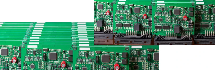
A true PCB partner should deliver more than just fabrication. Today’s projects demand a manufacturer who can produce a wide range of PCB types and also provide complete assembly, testing, and lifecycle support. Choosing wisely ensures not only reliable boards but also smoother production and faster time-to-market.
Key Capabilities to Look For
- Full PCB Range: From single-layer, double-layer to advanced multilayer PCBs, HDI, flexible, rigid-flex, metal-core, and high-frequency PCBs
- Assembly Expertise: Complete PCB assembly services including SMT, through-hole, mixed technology, and turnkey solutions
- Manufacturing Precision: Fine-line capability, microvia drilling, multiple surface finishes (ENIG, HASL, OSP), and advanced material handling
- Quality Systems and Test Coverage: Current site certificates where required, agreed IPC criteria, inspection/sampling, traceability and measured process controls; distinguish bare-board electrical tests from assembly functional tests
- Engineering Support: DFM analysis, prototyping, design consultation, and technical collaboration to optimize yield and reduce cost
Why HilPCB PCB Factory
Send HILPCB the board files, stackup, BOM where assembly is needed, quantities and required reports for a scoped quotation. Confirm the supplying site, fabrication and assembly processes, sourcing responsibilities and test limits for that order rather than inferring them from a general service label.
For a direct view of supported build types, engineering review, test scope, and quote inputs, see our PCB manufacturing and DFM review service page.
Cost Optimization Strategies
Factors Affecting PCB Manufacturing Cost
Design Complexity:
- Layer count and stackup complexity
- Via types (through-hole vs. microvia)
- Minimum trace width and spacing requirements
- Special features (blind vias, embedded components)
Material Selection:
- Standard FR4 vs. specialty materials
- Copper weight requirements
- Surface finish selection
- Thickness specifications
Volume and Timing:
- Prototype vs. production quantities
- Standard vs. expedited delivery
- Panel utilization efficiency
- Setup and tooling costs
Cost-Effective Manufacturing Tips
- Optimize Panel Utilization: Design PCB dimensions to fit efficiently on standard panel sizes
- Standardize Materials: Use common thicknesses and copper weights when possible
- Review Layer Count: Compare lower-layer alternatives only when routing, reference planes, power integrity and manufacturing yield remain acceptable
- Choose Appropriate Surface Finish: Balance performance requirements with cost considerations
- Plan for Volume: Consider long-term volume requirements in initial design decisions
Working with Your Manufacturing Partner
Successful Project Management
Clear Communication:
- Provide complete specifications and requirements
- Establish clear timelines and milestones
- Maintain regular project status updates
- Document all changes and approvals
Design Collaboration:
- Leverage manufacturer's DFM expertise
- Consider manufacturing constraints early in design
- Review and approve prototypes before production
- Plan for testing and validation requirements
From Design to Production
The transition from custom circuit board design to manufacturing requires careful planning:
- Design Finalization: Complete electrical and mechanical design validation
- Prototype Phase: Build and test prototypes to validate design
- Production Preparation: Finalize specifications and manufacturing documentation
- Manufacturing: Execute production with quality monitoring
- Assembly Planning: Coordinate with circuit board assembly services
Best Practices for Selecting a Circuit Board Manufacturing Company
When evaluating circuit board manufacturing options, consider the total value proposition beyond just price. The right manufacturing partner becomes an extension of your engineering team, contributing to product success through:
- Quality Excellence: Consistent, reliable products that enhance your reputation
- Technical Expertise: Engineering support that improves your designs
- Supply Chain Reliability: On-time delivery that supports your business goals
- Cost Optimization: Efficient processes that improve your profit margins
For guidance on selecting the right manufacturing approach, see our comprehensive guide on buying circuit boards.
Frequently Asked Questions About Circuit Board Manufacturing
How are circuit boards manufactured?
For a conventional plated-through multilayer board, the flow includes design review, inner-layer imaging/etching and inspection, lamination, drilling, hole preparation/metallization, copper build and outer-circuit formation, solder mask/legend, surface finish, profiling and final inspection/electrical test. Sequential-lamination HDI, flex and other constructions add or change steps.
How are design files turned into an accepted finished board?
The fabricator uses the approved artwork, drill data, stackup, material and drawing to generate tooling and process instructions. Agree finished dimensions, copper/plating, workmanship, electrical-test coverage and any impedance coupons before release. Inspection demonstrates the defined acceptance checks, not every possible circuit characteristic.
What is the difference between fabrication and assembly?
Fabrication produces the unpopulated board. Assembly adds component sourcing, solder-paste printing, placement, reflow or through-hole soldering, and the agreed inspection/programming/functional tests. The circuit board production flow and assembly scope should identify which party owns each operation.
What evidence should I request from a PCB manufacturing company?
Request current site-specific quality certificates where required, applicable UL recognition details, material/substance evidence, achievable construction limits and sample inspection/test records. Compare quotations using the same drawing, quantities, reports and change-control rules; a certificate alone does not guarantee yield or suitability.
Does every board use the same manufacturing process?
No. Single-sided boards, conventional multilayers, sequential HDI, flexible circuits and metal-core constructions have different drilling, bonding, metallization and handling routes. Match the process to the approved construction and validate changes before production.
Ready to Start Your PCB Manufacturing Project?
Provide the released design, material/stackup specification, quantity, required dates and acceptance plan so fabrication and any assembly can be quoted on a common basis.
Items to agree before release:
- ✅ Quality Evidence: Agree inspection coverage, sample sizes, acceptance limits and records
- ⚡ Schedule: Confirm material availability, tooling, test and delivery milestones
- 💰 Quotation: Separate tooling, unit cost, inspection, assembly and logistics
- 🔧 Engineering Review: Resolve DFM findings and control released changes
- 🏆 Supplier Evidence: Request relevant site certificates, build records and authorized references
Review a first article against the released drawing and reports, then define which material, process or design changes trigger renewed approval.
Contact our engineering team today to discuss your project requirements and discover how our advanced manufacturing capabilities can bring your innovative designs to life.
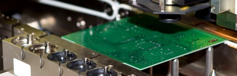
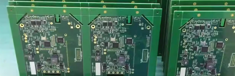
A green circuit board is a common solder-mask option. Select the actual mask chemistry, color, registration and inspection requirements rather than treating color as proof of board quality.