

Circuit board assembly is the manufacturing stage where a bare PCB becomes a functional electronic assembly. The process combines component sourcing, precision placement, soldering, inspection, and electrical testing to produce reliable products for consumer electronics, industrial equipment, medical devices, automotive systems, and other applications. For the full path from bare board to finished product, see our electronics assembly overview.
Professional PCB assembly services help engineers move from prototype designs to repeatable production by combining automated equipment, controlled processes, and manufacturing expertise. A well-managed assembly process reduces defects, improves production yield, and ensures the final product meets electrical and mechanical requirements.
Understanding PCB assembly methods helps designers create better custom circuit board design layouts, select appropriate components, and avoid manufacturing issues before production begins.
Understanding PCB Assembly Fundamentals
PCB assembly includes several controlled manufacturing steps that convert fabricated circuit boards into complete electronic products. Each stage affects final reliability, from component preparation to solder joint formation and functional testing. The difference between the bare board and the finished assembly is explained in PCA vs PCB.
A typical PCB assembly workflow includes:
- Component inspection and preparation
- Solder paste printing
- Surface mount component placement
- Through-hole component insertion
- Reflow or wave soldering
- Automated inspection
- Electrical testing
- Final quality verification
Modern assembly facilities use automated equipment such as pick-and-place machines, solder paste inspection systems, reflow ovens, automated optical inspection (AOI), and X-ray inspection systems. These technologies provide repeatable results for both prototype builds and high-volume manufacturing.
Successful assembly starts with manufacturing-aware design decisions. Component package selection, PCB footprint accuracy, thermal management, board stackup, and test point placement all influence assembly efficiency and product reliability. Close coordination between PCB design and circuit board manufacturing processes creates a smoother transition from bare board fabrication to finished assemblies.
Assembly Process Overview
Component Preparation
Inspection, testing, and preparation of components for assembly
Solder Paste Application
Precise stencil printing of solder paste onto PCB pads
Component Placement
High-precision automated placement of surface mount components
Reflow Soldering
Controlled heating process to form permanent solder joints
Surface Mount Technology (SMT) Assembly
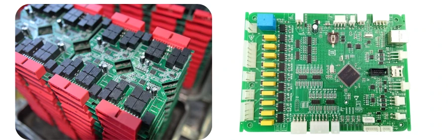
Surface Mount Technology (SMT) is the primary assembly method used for modern electronic products. SMT components are mounted directly onto circuit board surface pads instead of being installed through drilled holes.
The SMT process begins with solder paste printing. A precision stencil applies controlled amounts of solder paste to PCB pads. Paste thickness, alignment, and volume must remain consistent to prevent defects such as insufficient solder, solder bridging, or weak joints.
After printing, automated inspection verifies solder paste coverage and registration. Pick-and-place machines then position surface mount components with high accuracy. Machine vision systems confirm component orientation, polarity, and placement before the PCB enters the reflow process.
During reflow soldering, the PCB passes through a controlled temperature profile that melts the solder paste and forms permanent electrical connections. The profile must match the solder alloy, PCB materials, and component temperature limits to prevent damage and ensure reliable solder joints.
SMT Assembly Capabilities
Fine Pitch Components: Supporting advanced packages with pitches down to 0.3mm for high-density integrated circuits.
Micro Components: Installing 01005 and smaller passive components used in compact electronic designs.
High Pin Count Devices: Handling BGA, QFN, and other advanced semiconductor packages.
Mixed Technology: Combining SMT components with through-hole components in the same PCB assembly.
SMT assembly enables smaller product footprints, faster automated production, and improved repeatability. However, successful SMT manufacturing depends on accurate PCB footprints, proper component selection, and controlled production parameters.
Through-Hole Assembly and Mixed Technology
Through-hole assembly remains important for components that require mechanical strength, high current capacity, or additional durability. The process inserts component leads through drilled PCB holes and solders them to copper pads on the opposite side of the board. For a closer comparison of THT component and process choices, see the through-hole assembly guide.
Wave soldering is commonly used for high-volume through-hole production. The assembled PCB moves across a controlled wave of molten solder that creates connections between component leads and PCB pads.
Selective soldering provides more precise control for mixed-technology boards. It allows manufacturers to solder specific through-hole areas without exposing the entire assembly to additional thermal stress.
Hand soldering is used for prototypes, repairs, modifications, and specialized components. Skilled technicians use controlled soldering temperatures and appropriate flux materials to create reliable connections while protecting nearby components.
Through-Hole Assembly Applications
Through-hole technology is commonly used in applications requiring strong mechanical connections. Examples include:
- Power connectors
- Large capacitors
- Transformers
- Relays
- Components exposed to vibration or mechanical stress
Mixed technology assemblies combine SMT and through-hole components on one PCB. These designs require careful process planning because components may experience multiple heating cycles during reflow and selective soldering operations.
For successful circuit board designs using through-hole components, engineers should consider hole diameter, pad size, component spacing, and thermal relief patterns. These design details directly affect solder quality, production yield, and long-term reliability.
Advanced Assembly Techniques and Technologies
Advanced electronic products require specialized assembly processes to support smaller form factors, higher performance, and increased component density. Technologies such as Ball Grid Array (BGA), Chip Scale Package (CSP), and System-in-Package (SiP) require precise placement and inspection methods.
BGA assembly creates unique inspection challenges because solder joints are located beneath the component package. X-ray inspection provides a non-destructive method for evaluating hidden connections and identifying defects such as solder voids, incomplete joints, or bridging.
Specialized Assembly Services
Flip Chip Assembly: Direct attachment of semiconductor chips to substrates for applications requiring shorter electrical paths and improved performance.
Wire Bonding: Creating electrical connections between semiconductor dies and package structures using fine wire interconnects.
Die Attach: Precisely positioning and bonding semiconductor dies for custom electronic packages.
Conformal Coating: Applying protective coatings to improve resistance against moisture, chemicals, dust, and harsh operating environments.
Component-on-Board (COB) assembly mounts bare semiconductor dies directly onto PCBs. This approach reduces package size and can improve electrical and thermal performance for specialized applications.
Flexible and rigid-flex PCB assemblies require additional manufacturing controls. Assembly fixtures must support flexible areas without creating stress that could damage the board or affect component placement accuracy.
Quality Control, Testing, and Design Optimization in PCB Assembly
Quality control ensures that assembled PCBs meet electrical, mechanical, and reliability requirements. Effective quality systems identify problems early, reduce rework, and improve manufacturing consistency.
The process begins with incoming inspection of components and materials. Manufacturers verify part numbers, specifications, and condition before components enter production.
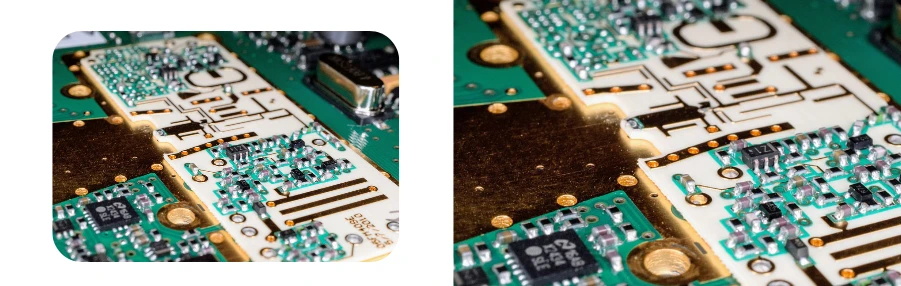
After solder paste printing, solder paste inspection checks paste volume, coverage, and alignment. Automated Optical Inspection (AOI) then verifies component placement, polarity, and visible solder joints.
Comprehensive Testing and Advanced Assurance
In-Circuit Testing (ICT) evaluates individual components and circuit connections using test fixtures. It can identify incorrect values, open circuits, short circuits, and assembly errors.
Functional testing verifies that the completed PCB operates according to product requirements. These tests simulate real operating conditions and confirm system-level performance.
Boundary scan testing uses JTAG interfaces to verify interconnections and component functionality without requiring direct access to every circuit node.
Additional inspection and testing methods include:
- X-ray Inspection: Non-destructive inspection of hidden solder joints, especially for BGA and advanced packages.
- Flying Probe Testing: Flexible fixture-free electrical testing for prototypes and low-volume production.
- Statistical Process Control (SPC): Monitoring manufacturing data to maintain consistent process performance.
For complete product validation, integration with circuit board testing services helps verify electrical performance, signal integrity, and reliability.
Assembly Design for Manufacturing (DFM)
Design for Manufacturing (DFM) improves PCB assembly reliability by addressing manufacturing requirements during the design phase. Early collaboration between engineers and manufacturers reduces redesign costs and improves production yield.
DFM Best Practices include:
- Standardization: Use common component packages to simplify sourcing, assembly setup, and inventory management.
- Accessibility: Provide sufficient clearance for inspection, testing, and component rework.
- Thermal Management: Manage heat-generating components to reduce thermal stress.
- Solder Joint Design: Optimize pad dimensions and thermal relief patterns for reliable solder connections.
Proper fiducial placement improves machine vision accuracy during automated assembly. Accessible test points simplify electrical testing and troubleshooting.
Engineers should also consider fabrication requirements such as via-in-pad structures, which may require specialized PCB processing to support reliable component attachment.
Choosing Professional PCB Assembly Services
Selecting a PCB assembly partner affects product quality, production cost, and time to market. The right manufacturer should provide reliable processes, engineering support, and scalable production capabilities.
When you compare PCB assembly services, use the same package, volume, inspection and test assumptions so supplier responses are comparable.
Key Evaluation Factors
When evaluating potential partners for buying circuit boards, consider:
- Technical Expertise: Verify experience with required package types, assembly technologies, and production volumes.
- Quality Systems: Look for established inspection procedures, IPC-A-610 practices, ISO-based quality management, and process monitoring.
- Supply Chain Management: Confirm component sourcing capabilities, supplier qualification methods, and inventory controls.
- Engineering Support: Evaluate available DFM reviews, test development, and manufacturing optimization services.
- Service Integration: Consider providers that combine procurement, assembly, inspection, testing, and fulfillment.
The best assembly partner depends on project requirements. Local manufacturers may provide faster communication and prototype support, while global production partners may offer cost advantages for larger volumes. For larger programs, our EMS manufacturing guide lists what to check in NPI, quality, and supply chain.
A structured transition from prototype builds to production manufacturing helps maintain consistency. Experienced assembly providers can apply prototype lessons to improve production processes and prevent recurring defects.
Complex designs, including multilayer circuit boards, require specialized assembly knowledge to manage component density, signal integrity requirements, and manufacturing constraints. Choosing a capable PCB assembly partner ensures the final product meets performance, reliability, and production goals.