Circuit board testing ensures electronic products meet design specifications, quality standards, and reliability requirements before reaching end users. Comprehensive testing programs combine automated inspection, electrical verification, and reliability validation to deliver products that perform consistently throughout their operational life. Professional testing services are essential for both prototyping phases and full production volumes, integrating seamlessly with circuit board manufacturing processes.
Understanding PCB Testing Fundamentals
PCB testing encompasses multiple disciplines from basic electrical continuity to complex system-level validation. Modern circuit boards integrate increasing functionality in smaller packages, demanding sophisticated testing approaches that verify both individual component performance and system-level interaction.
Testing begins during the circuit board manufacturing process and continues through circuit board assembly phases, providing quality gates that prevent defective products from advancing to subsequent process steps. The goal is detecting and correcting issues as early as possible to minimize costs and ensure reliability.
Testing Categories
Manufacturing Testing: Verifies boards meet manufacturing specifications
Assembly Testing: Validates component installation and solder joint quality
Functional Testing: Confirms circuits operate according to design requirements
Reliability Testing: Assesses long-term performance under stress conditions
Compliance Testing: Ensures products meet regulatory and safety standards
PCB Manufacturing Testing: Ensuring Quality from the Start
Before a printed circuit board (PCB) moves into the circuit board assembly stage, it undergoes a series of rigorous manufacturing tests. These tests ensure that the bare board is free of electrical, mechanical, and dimensional defects. By catching issues early, manufacturers reduce rework, improve yields, and deliver boards that meet strict industry standards.
1. Bare Board Electrical Testing (Continuity and Isolation)
One of the most critical steps is electrical testing of the bare board:
- Continuity Testing — Confirms that all intended connections exist by measuring resistance between nodes (typically <10 ohms). This prevents open circuits caused by etching errors or incomplete copper plating.
- Isolation Testing — Applies a high voltage (100—500V depending on application) between isolated nets to confirm insulation integrity. This prevents shorts that could be caused by etching residue, bridging, or drilling defects. Together, these tests verify the integrity of copper traces and via connections across the board.
2. Impedance Control Testing
High-speed digital and RF circuits require precise impedance matching. Time Domain Reflectometry (TDR) is used to measure the characteristic impedance of signal traces:
- Ensures controlled impedance for differential pairs and transmission lines.
- Maintains signal quality in multilayer circuit boards and high-frequency designs.
- Detects variations in trace width, dielectric thickness, or material inconsistencies that can degrade signal integrity.
Impedance testing is essential for boards used in telecommunications, data centers, automotive electronics, and aerospace applications.
3. Automated Optical Inspection (AOI) for Manufacturing
AOI systems provide a non-contact method of identifying visual and dimensional defects:
- Surface Defect Detection — Finds missing copper, trace breaks, over-etching, or solder mask misalignment.
- Dimensional Verification — Confirms board outline accuracy, hole diameters, pad locations, and feature-to-feature spacing.
- Silkscreen and Label Check — Ensures that reference designators and polarity markers are properly aligned and readable.
By comparing the manufactured board to digital design data, AOI ensures every panel meets tolerance before moving to assembly.
4. Mechanical and Dimensional Validation
In addition to electrical and optical checks, PCBs must meet mechanical standards:
- Board Thickness Measurement — Confirms compliance with design specs (important for press-fit connectors and controlled impedance).
- Warp and Twist Testing — Ensures the board remains flat within IPC tolerances, preventing assembly alignment issues.
- Hole Integrity — Checks drilled holes for size, roundness, and cleanliness, critical for through-hole plating and component insertion.
These validations guarantee that boards will perform reliably during downstream circuit board assembly and in end-use environments.
PCB Assembly Testing: Verifying Soldering and Component Accuracy
Once components are mounted on a circuit board, it is essential to verify the accuracy of placement and the integrity of solder joints. PCB assembly testing ensures that boards are fully functional, free of hidden defects, and ready for final system integration.
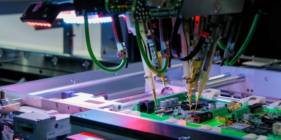
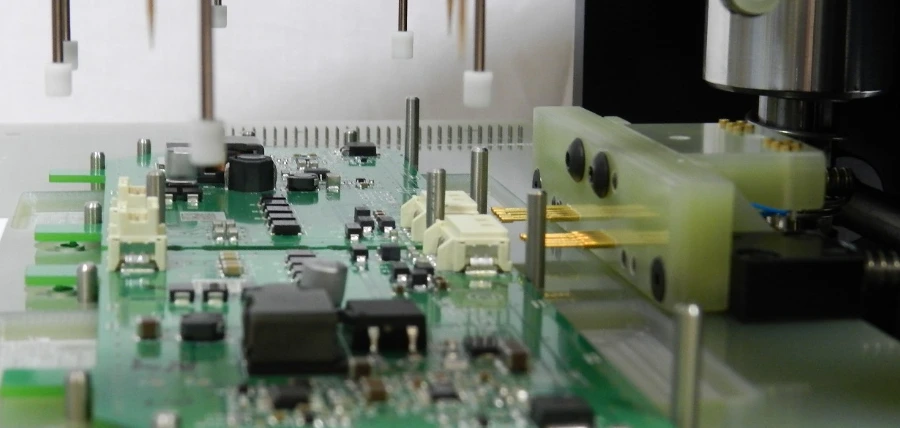
1. In-Circuit Testing (ICT)
ICT is one of the most widely used assembly tests. It verifies both component installation and circuit connections by applying electrical probes directly to test pads or nodes.
- Component Verification: Confirms resistor, capacitor, inductor values, and checks diodes, transistors, and IC pin functions.
- Solder Joint Integrity: Detects cold joints, open pins, or high-resistance paths.
- Coverage: Typically achieves 85—95% node coverage, making it highly effective for high-volume production.
- Limitations: Requires custom test fixtures, which may not be cost-effective for low-volume runs.
2. Boundary Scan Testing (JTAG)
For high-density boards where physical test access is limited, boundary scan testing provides excellent coverage.
- Method: Uses IEEE 1149.1 test access ports built into modern ICs.
- Applications: Ideal for testing processors, FPGAs, memories, and communication buses.
- Advantages: No physical probes required, reducing risk of mechanical damage.
- Limitations: Limited effectiveness for analog circuits or components without JTAG support.
3. Automated Optical Inspection (AOI) for Assembly
AOI plays a crucial role in visual verification after soldering. High-resolution cameras scan assembled boards and compare images to reference data.
- Checks Component Placement: Confirms part presence, orientation, polarity, and correct values.
- Evaluates Solder Joints: Inspects fillet shape, pad coverage, bridging, and solder quantity.
- Benefits: Provides fast, non-contact inspection, suitable for every production panel.
4. X-Ray Inspection (AXI)
For packages with hidden connections, such as BGAs, QFNs, and CSPs, X-ray inspection is indispensable.
- Hidden Joint Analysis: Detects voids, incomplete solder fills, and bridging under components.
- Via Fill Quality: Confirms whether filled or capped vias meet design specifications.
- Reliability Insight: Identifies defects invisible to AOI or ICT, preventing field failures.
5. Functional Testing of Assemblies
While ICT and AOI confirm physical integrity, functional testing verifies real-world operation:
- Ensures correct power-up sequences, voltage levels, and signal response.
- Simulates application conditions to confirm that assembled boards meet performance requirements.
- Detects issues that may not appear in structural tests, such as timing errors or firmware-related faults.
Functional and Reliability Testing: Proving Real-World Performance
Functional testing simulates real-world application conditions, ensuring boards operate exactly as designed.
- System-Level Functional Testing — Validates power-up, signal response, communication protocols, and performance benchmarks.
- Environmental Stress Testing — Boards are tested under temperature cycling, humidity, and vibration to confirm durability in harsh conditions.
- Burn-In Testing — Extended operation under elevated stress identifies early failures, improving long-term field reliability.
- Signal Integrity Analysis — Using time- and frequency-domain tools, we measure jitter, eye diagrams, crosstalk, and EMC pre-compliance for high-speed designs.
This combination of tests provides assurance that products will perform consistently over their expected lifespan.
Why Choose a China PCB Factory with Complete Testing Services
When selecting a PCB manufacturer for buying circuit boards, testing capability is a key factor. Highleap PCB Factory offers:
- Full manufacturing and assembly testing under IPC and ISO standards.
- Advanced inspection tools including AOI, X-ray, ICT, boundary scan, and impedance control.
- Support for prototypes through high-volume production.
- Seamless integration with custom circuit board design and circuit board manufacturing.
- Cost-effective solutions without compromising quality.
By combining manufacturing testing, assembly testing, functional testing, and reliability testing, we provide customers with one-stop solutions that reduce risk and improve time-to-market.
If you are searching for a China PCB factory that can provide complete testing services, Highleap PCB Factory is your trusted partner.