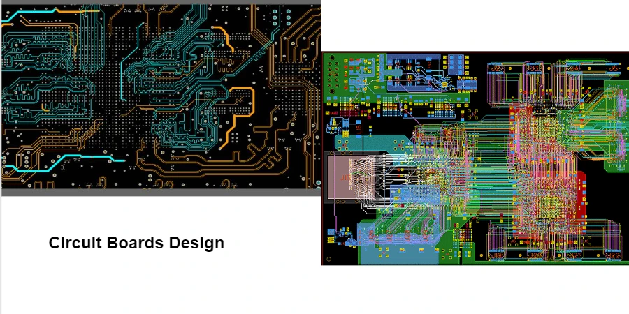
Custom circuit board design transforms electronic concepts into manufacturable products. Success requires balancing electrical performance, mechanical constraints, manufacturing requirements, and cost considerations. This comprehensive guide explores professional PCB design practices from initial planning through design validation, ensuring seamless integration with circuit board manufacturing and circuit board assembly processes.
Fundamentals of Custom PCB Design
Custom circuit board design begins with understanding project requirements and translating them into physical layouts. Modern PCBs integrate complex functionality in minimal space while meeting stringent performance requirements.
Effective design requires multidisciplinary expertise spanning electrical engineering, mechanical design, thermal management, and manufacturing processes. The goal is creating boards that perform reliably while remaining cost-effective to produce and suitable for efficient circuit board assembly.
Design Process Overview
Requirements Analysis: Define electrical, mechanical, environmental, and cost requirements
Schematic Design: Create detailed circuit schematics with component specifications
PCB Layout: Transform schematics into physical board layouts
Design Verification: Validate design through simulation and analysis
Prototype Testing: Build and test physical prototypes
Production Optimization: Refine design for manufacturing efficiency
Design Expertise Areas
High-Speed Design
Signal integrity analysis, controlled impedance, crosstalk minimization, and timing optimization for high-frequency applications.
Thermal Management
Heat dissipation strategies, thermal vias, copper pours, and component placement for optimal temperature control.
Mechanical Integration
3D modeling, connector placement, mounting strategies, and mechanical stress analysis for robust designs.
DFM Optimization
Design for manufacturing analysis, cost optimization, yield improvement, and production scalability planning.
Key Considerations for Effective PCB Design and Manufacturing
When designing custom PCBs for circuit board manufacturing, careful attention to the schematic, component selection, stackup design, and layout are essential to ensuring performance, reliability, and manufacturability. Here's what you need to know:
Schematic Design and Component Selection
The foundation of any PCB is its schematic design. A well-organized circuit layout ensures that signals flow efficiently and that power is distributed effectively across the board. It is crucial to define the signal flow logically, plan power distribution with decoupling strategies, and define input/output interfaces clearly.
Component selection is equally important. Choosing the right components based on electrical specifications and ensuring they fit mechanically into the design are essential. You must also consider cost and availability, as well as thermal management to ensure long-term reliability under operational stress.
PCB Stackup Design
The stackup design determines the number of layers and material types used in your PCB, directly affecting signal integrity and power distribution. For complex designs, multilayer circuit boards provide enhanced routing density and better electromagnetic compatibility. The key components of a stackup include signal layers for high-speed traces, power planes for efficient distribution, and ground planes for noise reduction.
Material selection plays a critical role, particularly when it comes to the dielectric properties that control impedance and signal propagation. Thermal properties of the material also ensure efficient heat dissipation, while balancing cost considerations helps maintain budget and performance goals.
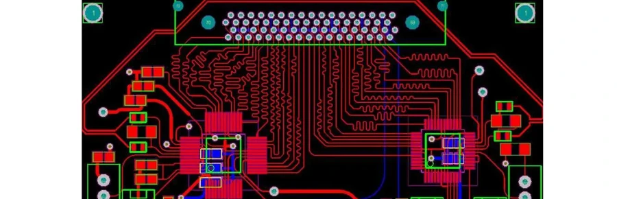
Layout Design and Routing
Effective component placement is the heart of PCB layout design. Components should be placed strategically to minimize signal path length, manage thermal distribution, and meet manufacturing constraints. Connector locations and mechanical interfaces must also be taken into account to ensure the board is both functional and easy to assemble.
Routing techniques are critical for high-speed designs. Controlled impedance, length matching, and minimizing vias are key considerations in high-speed routing. For mixed-signal designs, proper isolation between analog and digital circuits reduces noise and ensures signal integrity. Additionally, routing power and ground effectively ensures a low-impedance path with sufficient current capacity.
Ensuring PCB Performance: Signal Integrity, Power Distribution, and Thermal Management
To achieve high-performance PCBs, addressing signal integrity, power distribution, and thermal management is critical, especially in high-speed and complex designs.
Signal Integrity
Impedance control is essential to match trace impedance to system requirements, minimizing signal loss. Differential pairs should be routed with consistent spacing for clarity, and via design must minimize discontinuities. Timing analysis ensures correct signal propagation, low clock skew, and proper setup and hold margins. Effective noise management, including crosstalk reduction and EMI/EMC compliance, is vital to maintain data integrity.
Power Distribution
A well-designed power plane ensures efficient current distribution with minimal voltage drop. Decoupling capacitors should be strategically placed for noise reduction, while voltage regulation ensures stable power delivery. Proper monitoring helps safeguard circuits from power fluctuations.
Thermal Management
Effective heat dissipation is achieved through thermal vias and copper pours. Components should be placed to avoid hot spots, with thermal analysis identifying areas for additional cooling. Proper thermal modeling ensures the PCB operates within safe temperature limits, while cooling solutions like heat sinks enhance performance.
Ensuring a Seamless PCB Design and Production Process: DRC, DFM, and Prototyping
When designing custom PCBs for circuit board manufacturing, optimizing the design for manufacturability, reliability, and performance is essential. By using Design Rule Checking (DRC), Design for Manufacturing (DFM), and prototyping and testing, you can ensure a smooth transition from concept to finished product. Here's how each step plays a crucial role:
Design Rule Checking (DRC)
DRC ensures that your PCB design is not only functional but also manufacturable. Automated checks in electrical rules verify connectivity, clearance, and via sizes, ensuring there are no issues that could affect performance or manufacturability. Manufacturing rules check key aspects like trace width, drill sizes, and solder mask openings, preventing problems during production. Assembly rules focus on the correct placement of components and providing clear markings for assembly and testing.
- Electrical Rules: Ensure proper connectivity, clearance, and via sizes.
- Manufacturing Rules: Verify trace width, drill sizes, and solder mask requirements.
- Assembly Rules: Check component placement, silkscreen readability, and test point accessibility.
Design for Manufacturing (DFM)
DFM analysis optimizes your PCB design to ensure it is cost-effective and easy to manufacture. This includes standardizing processes to match manufacturing capabilities, optimizing for yield by reducing features that may complicate production, and eliminating unnecessary complexity and exotic materials to minimize costs. In addition, assembly considerations ensure that components are placed for efficient circuit board assembly, with adequate access for rework and testing.
- Manufacturability Guidelines: Design within standard manufacturing capabilities to improve yield and reduce costs.
- Assembly Considerations: Optimize for efficient component orientation, easy rework access, and test point availability.
Prototype Development and Testing
Prototyping is an essential step in validating your design before full-scale production. Early prototype development helps test and refine your design to ensure it meets all functionality and performance specifications. During the prototype planning phase, define the testing objectives, necessary test equipment, and plan for iterative improvements based on test results. Design validation includes functional testing to verify that all circuits work as expected, performance testing to measure key parameters, and environmental testing to ensure the board can withstand real-world conditions.
- Prototype Planning: Define testing goals and prepare for iterative design adjustments.
- Design Validation: Ensure functional, performance, and environmental requirements are met.
For comprehensive validation, consider integrating circuit board testing services to verify electrical parameters, signal integrity, and reliability under various operating conditions.
By integrating DRC, DFM, and thorough prototyping and testing, you can reduce errors, streamline the manufacturing process, and ensure that your final product performs reliably and meets industry standards. Highleap PCB Factory provides comprehensive services from design validation through to full-scale production, helping you turn your ideas into high-quality, manufacturable PCBs.
Advanced PCB Design and Optimization for High-Quality Production
High-quality circuit board manufacturing starts with the right design approach. By combining smart layout planning, reliable materials, and efficient processes, you can reduce production costs while ensuring long-term performance.
Key Focus Areas:
- Design Efficiency: Use HDI, rigid-flex, or high-frequency PCB techniques only when required, balancing performance with cost.
- Built-in Reliability: Apply proper signal routing, thermal management, and compliance checks early in the design stage.
- Cost Control: Optimize layer count, board size, and material selection to keep pricing competitive while maintaining quality.
At Highleap PCB Factory, we support you from custom circuit board designthrough mass production, offering one-stop circuit board assembly and full testing. For a smarter sourcing strategy, see our guide on buying circuit boards.
Why Choose Highleap PCB Factory for Your Custom Circuit Board Design?
When it comes to circuit board design, choosing the right partner is essential for ensuring a successful, high-performance product. At Highleap PCB Factory, we specialize in both circuit board manufacturing and circuit board assembly, providing end-to-end solutions that guarantee efficiency and reliability for your project.
Expertise and Capabilities You Can Rely On
- Industry-Leading Design Experience: Our team has extensive experience in custom circuit board design for a wide range of industries, allowing us to handle diverse project requirements with precision.
- Advanced Tools and Technology: We use state-of-the-art CAD tools and simulation capabilities to ensure your design is optimized for performance and manufacturability, saving both time and costs.
- Manufacturing and Assembly Expertise: As a leading PCB manufacturer and assembler, we understand the intricacies of production and assembly, ensuring your design is production-ready and cost-effective.
Comprehensive Service from Design to Assembly
- Clear Communication and Project Management: We prioritize clear communication, providing you with detailed updates throughout the design and assembly process to ensure your project stays on schedule.
- Thorough Documentation: We offer complete design documentation and deliverables, making the transition from design to circuit board assembly seamless and transparent.
- Ongoing Support: From design to final assembly, we provide comprehensive support throughout the production ramp-up, ensuring that your circuit boards are ready for mass production without any issues.
Why Partner with Highleap PCB Factory?
Effective circuit board design is about balancing electrical performance, mechanical constraints, and manufacturing efficiency. At Highleap PCB Factory, we offer more than just design—we provide full-service circuit board manufacturing and assembly under one roof, ensuring consistency and quality from start to finish. Our experienced team combines advanced design tools, industry knowledge, and manufacturing expertise to deliver high-quality solutions tailored to your specific needs.
Partner with us today to transform your designs into fully functional, reliable circuit boards with seamless circuit board assembly and manufacturing.