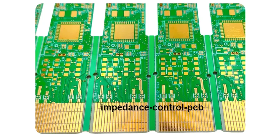
When a next-generation 5G base station fails its first compliance test, the culprit is often not the chipset or the software—it’s the PCB. Impedance mismatches create standing waves, reflections, and unwanted harmonics that cripple RF and microwave performance. For high-frequency designs, precise impedance control is not optional; it’s the foundation of reliable operation and regulatory compliance.
At Highleap PCB Factory (HILPCB), we specialize in RF and microwave PCB manufacturing with ±5Ω impedance accuracy. Our engineering process eliminates variability before your design reaches the test bench, ensuring optimal signal integrity for 5G, aerospace, defense, and other critical applications.
The Physics Behind Impedance Control
Understanding impedance control starts with recognizing that every PCB trace behaves as a transmission line at frequencies where signal wavelengths approach trace dimensions. For modern digital systems operating at multi-gigahertz frequencies, even short traces exhibit transmission line behavior requiring careful impedance management.
Characteristic Impedance Fundamentals: The relationship between trace geometry and impedance follows well-established electromagnetic principles. For microstrip traces, characteristic impedance depends on trace width, copper thickness, substrate height, and dielectric constant. Small variations in any parameter can significantly impact the final impedance value, making manufacturing control essential for consistent results.
Material Properties Impact: PCB substrate materials exhibit frequency-dependent dielectric properties that affect impedance stability across operating bandwidths. Standard FR4 materials provide adequate performance for applications below 5GHz, while specialized low-loss materials become necessary for millimeter-wave applications. Our material selection process considers both electrical performance and manufacturing compatibility.
Temperature Coefficient Effects: Impedance stability across temperature ranges depends on thermal expansion characteristics of both substrate and copper conductors. High-Tg PCB materials provide better dimensional stability, while proper thermal management prevents impedance drift during operation.
Manufacturing Process Excellence
Achieving consistent impedance control requires integrated manufacturing processes that monitor and control every variable affecting final electrical performance.
Statistical Process Control Implementation: Our impedance control manufacturing uses comprehensive SPC systems monitoring trace width, copper thickness, and dielectric height across every production panel. Real-time data collection enables immediate process adjustments, maintaining impedance within ±5% specifications consistently.
Advanced Copper Plating Control: Electroplating uniformity directly affects trace resistance and impedance characteristics. Our automated plating systems use current density optimization and real-time thickness monitoring to achieve uniform copper distribution, even in complex HDI PCB designs with high aspect ratio vias.
Precision Etching Techniques: Trace width control during etching determines final impedance accuracy. Our enhanced etching processes use real-time monitoring of etch rate uniformity with automatic chemistry adjustments maintaining consistent trace profiles across entire panel areas.
High-Speed Digital System Applications
Modern processors and communication systems push frequency boundaries that make impedance control critical for basic functionality, not just optimal performance.
Processor Interface Design: Next-generation CPUs operate at clock frequencies approaching 10GHz with edge rates in the sub-100 picosecond range. At these speeds, every trace behaves as a transmission line where impedance mismatches cause reflections that can corrupt data or create timing violations. DDR5 memory interfaces exemplify this challenge, requiring 50Ω single-ended impedance control within ±7% to maintain timing margins across all operating conditions.
SerDes Channel Optimization: Multi-gigabit serial interfaces like 25G/100G Ethernet and PCIe Gen 5 use advanced signaling techniques that demand exceptional impedance accuracy. Channel equalization and forward error correction can compensate for some channel impairments, but consistent impedance provides the foundation for reliable high-speed communication.
Power Delivery Network Integration: High-performance processors require sophisticated power delivery systems that must coexist with sensitive high-speed signals. Power plane impedance affects signal integrity through ground bounce and simultaneous switching noise. Our multilayer PCB stackup designs optimize both signal impedance and power delivery impedance for maximum system performance.
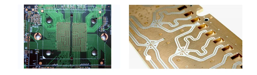
RF & Microwave PCB Engineering for Optimal Signal Integrity
RF and microwave PCB design demands the most stringent impedance control, as even minor deviations can cause measurable loss, reflection, and distortion.
50Ω System Integrity
The industry-standard 50Ω impedance offers the optimal balance between power handling and attenuation. Achieving this consistently requires precise control over trace dimensions, dielectric properties, and fabrication tolerances. Our processes maintain ±2Ω accuracy across varied stack-ups, ensuring maximum power transfer and signal fidelity.
Optimized Transmission Line Topologies
Common RF geometries include microstrip, stripline, and coplanar waveguide:
- Microstrip – Simplifies component access and tuning.
- Stripline – Offers superior isolation within multilayer structures.
- Coplanar Waveguide – Provides stable impedance with adjacent ground references.
**Controlled Via Transitions **
Layer changes introduce inductive and capacitive discontinuities that degrade RF performance. We employ impedance modeling, stub elimination via back-drilling, and optimized pad/via geometry to minimize insertion loss and reflections.
Precision Connector Interfaces
From PCB trace to coaxial interface, impedance continuity is critical. Our connector footprint engineering ensures matched impedance, minimal parasitics, and mechanical robustness for repeatable high-frequency performance.
Testing and Validation Protocols
Comprehensive testing validates impedance control performance across all manufacturing variables and operating conditions.
Time Domain Reflectometry (TDR): TDR measurements provide the primary method for impedance validation, measuring characteristic impedance along trace lengths with resolution sufficient to identify localized impedance variations. Our calibrated TDR systems operate across frequency ranges from DC to 40GHz with measurement uncertainty traceable to national standards.
Network Analyzer Characterization: Vector network analyzer measurements complement TDR testing by characterizing impedance behavior across wide frequency ranges. S-parameter measurements validate insertion loss, return loss, and impedance consistency for high-frequency applications where frequency-dependent effects become significant.
Production Test Coupon Design: Every impedance control panel includes dedicated test coupons that replicate critical trace geometries and stackup configurations. Test coupons undergo identical manufacturing processes as functional PCBs, providing accurate representation of actual electrical performance across all production variables.
Our SMT assembly capabilities ensure precise component placement for impedance-critical applications, while rigid-flex PCB technology extends impedance control to complex three-dimensional assemblies.
Frequently Asked Questions
Q: What impedance tolerance can you achieve in production? We routinely achieve ±5% impedance tolerance for standard applications, with ±2Ω capability for critical RF applications through advanced process control and premium material selection.
Q: How do you validate impedance control during manufacturing? Every production panel includes impedance test coupons measured using calibrated TDR equipment, with complete documentation provided for traceability and quality assurance.
Q: Can impedance be controlled on flexible PCBs? Yes, flex PCB designs can achieve controlled impedance using specialized flexible dielectric materials and precise conductor geometry control.
Q: What's the impact of temperature on impedance stability? Material selection significantly affects temperature stability. Standard FR4 shows ~3% impedance change over automotive temperature ranges, while specialized materials provide better stability for critical applications.
Q: How early should impedance requirements be established? Impedance requirements should be defined during initial stackup design to ensure manufacturable solutions and prevent costly design revisions.
Q: What test methods validate impedance accuracy? We use both TDR and network analyzer measurements on production test coupons to validate impedance performance and characterize frequency response across your operating bandwidth.