In the era of ubiquitous wireless connectivity, high-frequency PCB antenna design has become a critical skill for engineers developing everything from 5G smartphones to IoT sensors. Modern antenna design must balance size constraints, performance requirements, and manufacturing costs while operating across frequencies from sub-GHz to millimeter-wave bands. This comprehensive guide explores the principles, techniques, and practical considerations for designing high-performance PCB antennas that meet the demanding requirements of today's wireless systems.
1. Fundamentals of PCB Antenna Design for High-frequency Applications
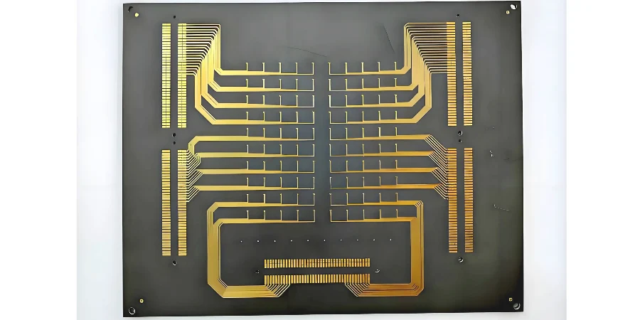
PCB antennas offer the unique advantage of being integrated directly onto the circuit board, eliminating the need for external antennas and reducing overall system cost. At high frequencies, the antenna becomes an extension of the RF circuit, requiring careful consideration of materials, geometry, and surrounding environment.
The key parameters that define antenna performance include resonant frequency, bandwidth, radiation pattern, gain, and efficiency. For a typical patch antenna on FR4 substrate operating at 2.4 GHz, the wavelength in the dielectric is approximately 60mm, making quarter-wave structures feasible even in compact devices. However, as frequency increases to 28 GHz for 5G applications, wavelengths shrink to just 5mm in substrate, demanding extreme precision in manufacturing.
Material selection critically impacts antenna performance. Low-loss substrates like Rogers RO4003C (εr=3.38, tanδ=0.0027) provide superior efficiency compared to standard FR4, particularly above 1 GHz. The dielectric constant affects antenna size—higher εr enables smaller antennas but reduces bandwidth and efficiency. For high-speed PCB applications combining digital processing with wireless connectivity, hybrid stackups using different materials for antenna and digital sections optimize both performance and cost.
2. Types of High-frequency PCB Antennas and Their Applications
Different antenna types suit various applications based on frequency, size constraints, and performance requirements. Understanding the trade-offs enables optimal selection for specific use cases.
Microstrip Patch Antennas
Patch antennas remain the most popular choice for PCB integration due to their low profile and ease of manufacturing. A rectangular patch antenna's dimensions are approximately λ/2 × λ/2, where λ is the wavelength in the substrate. For a 5.8 GHz WiFi antenna on Rogers RO4350B (εr=3.48):
- Patch width: 16.2mm for optimal radiation
- Patch length: 15.8mm accounting for fringing fields
- Ground plane: Minimum 3× patch dimensions
- Typical gain: 6-8 dBi
Enhanced designs incorporate:
- Stacked patches for increased bandwidth (10-15% achievable)
- Parasitic elements for beam steering
- Slot coupling for improved isolation
- Air gaps between substrate layers for efficiency
Inverted-F and Monopole Antennas
For compact devices requiring omnidirectional patterns, inverted-F antennas (IFA) and printed monopoles offer excellent solutions. These antennas are particularly suited for:
- Bluetooth/WiFi modules requiring 360° coverage
- IoT sensors with size constraints
- Wearable devices needing conformal designs
Design considerations include:
- Ground plane size affects resonant frequency (20% variation typical)
- Feeding point location controls impedance (50Ω matching critical)
- Meandering increases electrical length in limited space
- Keep-out zones prevent detuning from nearby components
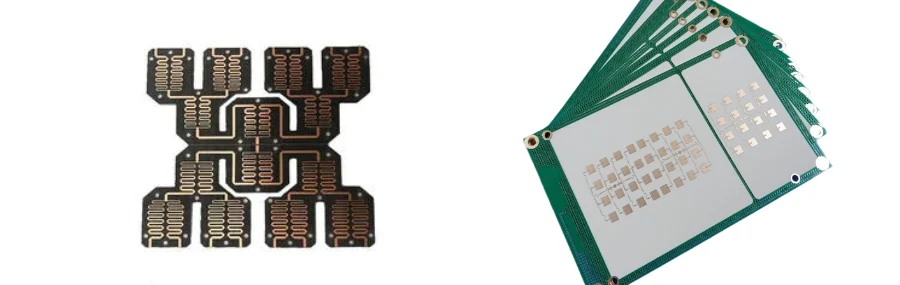
MIMO and Array Antennas
Modern wireless standards like 5G and WiFi 6 require multiple-input multiple-output (MIMO) configurations. Array antennas for 5G PCB applications present unique challenges:
- Element spacing: 0.5λ minimum for decorrelation
- Mutual coupling: <-15dB between elements
- Phase control: ±5° accuracy for beamforming
- Feed networks: Equal amplitude/phase distribution
Corporate feed networks using Wilkinson dividers ensure proper power distribution while maintaining isolation between elements.
3. Design Methodology for High-Performance PCB Antennas
Successful antenna design follows a systematic approach from specification through validation. This methodology ensures first-pass success and optimal performance.
Specification and Constraint Analysis
Begin by defining clear requirements:
- Frequency bands: Center frequency and bandwidth
- Radiation pattern: Directional vs omnidirectional
- Gain target: Accounting for system link budget
- Size constraints: Available PCB area
- Environmental: Temperature, humidity effects
- Regulatory: FCC/CE compliance requirements
Electromagnetic Simulation and Optimization
Modern antenna design relies heavily on 3D electromagnetic simulation. Tools like CST Studio Suite, Ansys HFSS, and Keysight ADS enable accurate prediction of antenna performance before fabrication.
Simulation workflow:
- Initial geometry based on analytical formulas
- Material definition including accurate εr and tanδ
- Mesh refinement for λ/20 minimum resolution
- Parametric sweep optimizing dimensions
- Environmental effects including enclosure and components
- Tolerance analysis for manufacturing variations
Key metrics to optimize:
- S11 <-10dB across operating band
- Radiation efficiency >70% (>50% minimum)
- Pattern stability across frequency
- Specific absorption rate (SAR) for body-worn devices
Manufacturing Considerations
PCB antenna manufacturing requires tighter tolerances than typical circuit boards. Critical parameters include:
- Etching tolerance: ±25μm affects resonant frequency
- Substrate thickness: ±10% variation shifts frequency 2-3%
- Copper roughness: Impacts efficiency at mmWave
- Solder mask: Avoid over antenna areas (shifts frequency)
- Via placement: Precise positioning for impedance matching
For multilayer PCB antennas, registration between layers must maintain ±50μm to prevent pattern distortion.
4. Advanced Techniques for mmWave Antenna Integration
As wireless systems migrate to millimeter-wave frequencies for 5G and automotive radar, antenna design becomes increasingly challenging. At 28 GHz and above, traditional approaches fail due to excessive losses and manufacturing tolerances.
Antenna-in-Package (AiP) Solutions
AiP technology integrates antennas within the IC package, minimizing losses and enabling highly integrated solutions. Design considerations include:
- Substrate selection: Low-loss organic or LTCC materials
- Via transitions: Optimized for minimal reflection
- Heat dissipation: Thermal vias under active circuits
- EMI shielding: Compartmentalization between RF blocks
Our AiP solutions achieve:
- Efficiency >60% at 28 GHz
- Bandwidth >2 GHz for 5G n257/n258 bands
- Beam steering ±60° for phased arrays
- Integration with transceivers and front-end modules
Substrate Integrated Waveguide (SIW) Antennas
SIW technology enables low-loss antenna designs above 20 GHz using standard PCB processes. Via fences create waveguide-like structures with excellent performance:
- Loss reduction: 50% compared to microstrip at 60 GHz
- High isolation: >40dB between adjacent elements
- Power handling: Superior to planar structures
- Integration: Compatible with passive components
Design rules:
- Via diameter: d < λg/5
- Via pitch: p < 2d
- SIW width: Follows rectangular waveguide formulas
- Transitions: Tapered microstrip-to-SIW
5. Testing and Validation of PCB Antennas
Comprehensive testing ensures antennas meet specifications across operating conditions. Our validation process combines simulation correlation, prototype measurements, and production testing.
Anechoic Chamber Measurements
Professional antenna characterization requires anechoic chamber testing:
- 3D radiation patterns with 1° angular resolution
- Gain measurement using gain comparison method
- Efficiency calculation from pattern integration
- Polarization including cross-pol levels
- Near-field to far-field transformation for large arrays
Our compact antenna test range supports frequencies from 700 MHz to 90 GHz with measurement uncertainty <0.5 dB.
Network Analyzer Testing
S-parameter measurements validate impedance matching:
- Return loss across frequency and temperature
- Active S-parameters for MIMO configurations
- Time domain analysis for debugging
- Smith chart for matching network design
Production testing uses simplified setups:
- Single-point S11 measurement at center frequency
- Go/no-go testing with ±2 dB tolerance
- Statistical process control for trend monitoring
Over-the-Air (OTA) Performance
System-level testing evaluates complete wireless performance:
- Total Radiated Power (TRP)
- Total Isotropic Sensitivity (TIS)
- Error Vector Magnitude (EVM)
- Throughput testing
- Coexistence with other radios
These measurements ensure real-world performance meets expectations.
6. Why Choose HILPCB for PCB Antenna Design and Manufacturing
HILPCB combines antenna design expertise with advanced PCB manufacturing capabilities to deliver complete wireless solutions:
- Design Services: Full-wave simulation, optimization, and prototyping
- Materials: Complete inventory of low-loss RF substrates
- Manufacturing: ±25μm tolerance, controlled impedance ±5%
- Testing: Anechoic chamber, network analyzer, and OTA validation
- Integration: Complete RF front-end including filters and amplifiers
- Support: Design review, DFM optimization, and troubleshooting
Our engineers have successfully developed antennas for:
- 5G base stations and small cells (3.5/28/39 GHz)
- Automotive radar (24/77 GHz)
- WiFi 6/6E access points
- IoT sensors and wearables
- Satellite communications
7. Frequently Asked Questions (FAQ)
Q1: How does PCB substrate affect antenna performance?
A: Substrate dielectric constant determines antenna size (higher εr = smaller antenna), while loss tangent affects efficiency. Low-loss materials like Rogers RO4003C improve efficiency by 20-30% compared to FR4, especially above 1 GHz.
Q2: What's the minimum ground plane size for patch antennas?
A: Ground plane should extend at least λ/4 beyond patch edges for stable performance. Smaller ground planes shift resonant frequency up to 10% and distort radiation patterns. For 2.4 GHz on FR4, minimum ground plane is 60×60mm.
Q3: How do I reduce mutual coupling in MIMO antennas?
A: Maintain λ/2 spacing between elements, orient antennas orthogonally, use decoupling structures like slots or parasitic elements, and implement neutralization lines. Target <-15dB isolation for good MIMO performance.
Q4: Can I use FR4 for 5G millimeter-wave antennas?
A: FR4 exhibits excessive losses (>2 dB/cm) above 10 GHz, making it unsuitable for mmWave. Use low-loss materials like Rogers RO3003 (loss <0.5 dB/cm at 28 GHz) for acceptable efficiency.
Q5: How do nearby components affect antenna performance?
A: Metal components within λ/4 detune the antenna and distort patterns. Maintain 5-10mm keepout zones, use RF shields where necessary, and simulate with actual component placement for accurate predictions.
Q6: What's the typical efficiency for PCB antennas?
A: Well-designed PCB antennas achieve 70-85% efficiency on low-loss substrates, 50-70% on FR4. Efficiency decreases with frequency due to conductor and dielectric losses. Small antennas (<λ/10) rarely exceed 30% efficiency.
Ready to Start Your Antenna Design Project?
Our RF engineers specialize in developing high-performance PCB antennas for demanding wireless applications. Contact us for design consultation and manufacturing solutions.