Introduction
High-Frequency PCBs (HF PCBs) power today's most advanced technologies—from 5G communications and automotive radar to aerospace systems and high-speed computing. As devices push beyond conventional frequency limits, understanding HF PCB materials, design principles, manufacturing processes, and reliability testing becomes essential for both engineers and decision-makers.
This guide combines deep technical insights with practical implementation strategies, covering the 20 key topics essential for HF PCB success. It is designed to serve both engineers seeking technical knowledge and decision-makers ready to source high-performance boards.
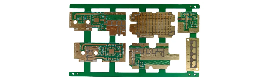
1. Materials and Layer Stackup for High-frequency PCBs
High-frequency PCB Materials
Selecting the right high-frequency PCB materials is the foundation of performance. Standard FR-4 struggles above 1 GHz due to high loss. Alternatives include:
- Rogers RO4000 / RO3000 series – Stable dielectric constant, low loss tangent.
- PTFE-based laminates – Excellent signal transmission but require special processing.
- Ceramic-filled composites – Low Dk, high mechanical stability.
Low dielectric constant (Dk) and low dissipation factor (Df) minimize signal delay and loss, directly affecting signal integrity.
High-frequency PCB Layer Stackup
HF PCB layer stackup controls impedance and EMI. Engineers arrange signal, power, and ground layers strategically:
- Signal layers adjacent to ground planes for impedance stability.
- Hybrid stackups (premium HF materials for signal layers, economical materials for others) to balance performance and cost.
- Shielding layers to isolate high-speed traces.
Proper stackup design is critical for high-frequency PCB impedance control and thermal management.
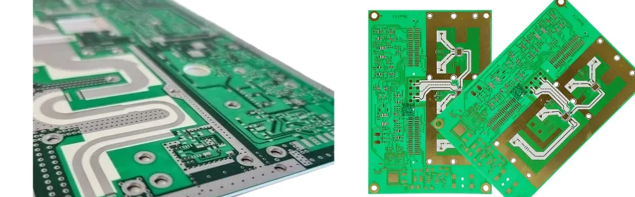
2. Design Principles, Impedance Control, and Power Delivery
High-frequency PCB Design Principles
HF PCB design treats every trace as a transmission line:
- Controlled trace widths and spacing to maintain target impedance (50Ω, 75Ω, 100Ω differential).
- Short, direct routing to reduce attenuation.
- Avoid right-angle bends to prevent reflections.
High-frequency PCB Impedance Control
Tight impedance tolerance (±5% or better) is achieved through:
- Simulation (HFSS, ADS) before fabrication.
- Adjusting trace width, dielectric thickness, and copper weight.
- Using test coupons during manufacturing.
High-frequency PCB Power Design
Power delivery must maintain low impedance from DC to GHz:
- Layered decoupling strategy (bulk → mid-band → ultra-low inductance caps).
- Star grounding to isolate noise-sensitive circuits.
- Wide copper pours for minimal voltage drop.
3. Signal Integrity and Common Issues
In high-frequency PCB design, signal integrity is one of the most critical performance factors. At GHz frequencies, even minor impedance mismatches can cause insertion and return loss, leading to reflections and reduced signal power. Crosstalk between adjacent traces and electromagnetic interference (EMI/RFI) from nearby sources can further distort waveforms, degrade bit error rates, and cause failures in high-speed communication systems. Maintaining consistent impedance, using proper via design, and ensuring continuous reference planes are fundamental to preserving signal quality.
Key Layout Strategies for Preserving Signal Integrity:
- Ground Planes: Provide stable return paths and reduce susceptibility to external noise.
- Via Fencing: Creates an electromagnetic barrier that minimizes coupling between high-speed traces.
- Controlled Trace Separation: Maintains spacing rules (e.g., 3W rule) to prevent crosstalk in parallel routing.
- Edge Plating and Shielding: Contain high-frequency energy within designated zones to meet EMC compliance.
However, signal integrity is not purely a matter of design—it is also affected by real-world manufacturing and environmental factors. Thermal performance degradation of 20–30% at high operating temperatures can alter dielectric constants, changing the intended impedance. Tight manufacturing tolerances are essential to prevent trace width or spacing variations that can introduce mismatches. Additionally, moisture absorption in certain laminates can increase loss tangent, detune RF circuits, and reduce reliability over time, making material choice and protective finishes a key part of maintaining long-term performance.
4. Manufacturing Process, Soldering, and Reliability Testing
High-frequency PCB Manufacturing Process
The high-frequency PCB manufacturing process involves far more precision than standard PCB fabrication due to the sensitivity of high-speed signals to dimensional variations and material inconsistencies. Each stage must maintain tight tolerances to preserve signal integrity and controlled impedance.
Key stages include:
Material Preparation and Handling HF PCB substrates—especially PTFE and ceramic-filled laminates—are moisture-sensitive and can absorb water vapor from the environment. Even 0.1% moisture absorption can impact dielectric properties, causing phase shifts and increased loss at GHz frequencies. Manufacturers use climate-controlled storage rooms and pre-bake laminates to drive out moisture before processing.
Layer Imaging and Etching Laser Direct Imaging (LDI) is preferred for fine-line accuracy and precise registration between layers. This process can achieve trace widths and spaces below 50 μm, critical for maintaining impedance and reducing crosstalk. High-frequency boards often have tighter etching tolerances, sometimes ±10% or better.
Drilling and Via Formation Laser-drilled microvias enable high-density interconnects (HDI) and shorter signal paths between layers. At high frequencies, via stub removal (back-drilling) is essential to avoid signal reflections. Staggered and stacked microvia designs are used to optimize signal integrity and mechanical strength.
Plating and Copper Deposition Uniform copper thickness ensures predictable impedance. Pulse plating techniques help maintain even copper distribution in microvias and narrow traces, reducing skin-effect-related losses at high frequencies.
Lamination and Alignment Multi-layer HF PCBs require precise layer-to-layer alignment (±25 μm or better). Laminating PTFE materials often requires lower temperatures and pressure profiles to prevent material deformation.
Statistical Process Control (SPC) Continuous monitoring of impedance test coupons, trace dimensions, and dielectric thickness ensures that final boards meet design targets. SPC systems flag variations early to avoid batch-wide failures.
High-frequency PCB Soldering Process
Assembly of HF PCBs must take into account the lower glass transition temperature (Tg) and mechanical properties of PTFE and other high-frequency materials.
Key considerations:
- Optimized Reflow Profiles: Gradual ramp-up and controlled cooling prevent warping and delamination. HF materials may require peak reflow temperatures 10–20°C lower than FR-4 to avoid substrate damage.
- Lead-free Solder Alloys: Alloys like SAC305 comply with RoHS while offering good wetting on gold, ENIG, or immersion silver finishes. Flux selection is also critical to avoid residue that could alter surface impedance.
- Component Placement Precision: High-frequency circuits often use small, sensitive RF components (e.g., 0201 capacitors, MMICs). Automated placement machines with ±30 μm accuracy are essential to ensure proper electrical performance.
High-frequency PCB Testing Methods & Reliability Testing
Testing and reliability validation are integral to HF PCB production. Even minor deviations can significantly affect performance at GHz frequencies.
Testing includes:
- Vector Network Analyzer (VNA): Measures S-parameters to determine insertion loss, return loss, and isolation. For example, a 0.2 dB/inch insertion loss target at 10 GHz may be required for aerospace radar boards.
- Time-Domain Reflectometry (TDR): Detects impedance discontinuities with sub-millimeter resolution, identifying defects like plating voids or trace width variations.
- Thermal Cycling: Simulates temperature fluctuations from -40°C to +125°C to ensure mechanical stability and consistent electrical performance.
- Vibration Testing: Especially important for automotive and aerospace applications to verify solder joint and via reliability under mechanical stress.
- Humidity and Salt Fog Testing: Evaluates corrosion resistance and dielectric stability in harsh environments.
- Near-field EMI Scanning: Maps radiated emissions and identifies potential coupling paths, helping designers implement targeted shielding and grounding improvements.
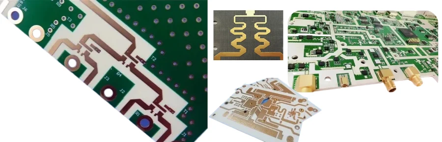
5. Packaging Types and Antenna Integration
High-frequency PCB Packaging Types
Popular packages:
- BGA – High I/O, lower inductance.
- QFN/LGA – Low profile, good thermal performance.
- Hermetic packages for aerospace and defense.
High-frequency PCB Antenna Design
Integrated antennas reduce component count:
- Microstrip patch antennas for GPS/Wi-Fi.
- Dipole/monopole antennas for IoT devices.
- Array antennas for radar and 5G beamforming.
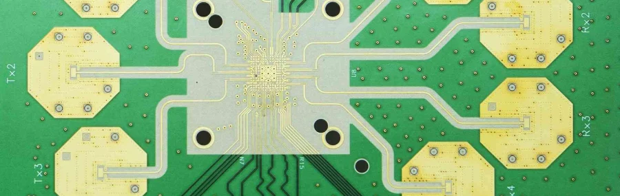
6. Applications: Microwave Systems and RF Circuits
Microwave Applications of High-frequency PCBs
High-frequency PCBs are critical in microwave and millimeter-wave applications where signal loss, impedance stability, and phase control are paramount.
Key application areas:
Automotive Radar (77–81 GHz) Used for adaptive cruise control, collision avoidance, and autonomous driving. These PCBs integrate antenna arrays, RF front-end modules, and signal processors on a compact multilayer board. Materials must have low Dk variation across temperature to ensure accurate target detection.
Aerospace and Defense Radar (>100 GHz) W-band (75–110 GHz) and higher-frequency radars require ultra-low-loss ceramic-filled PTFE for long-range detection and high-resolution imaging. Such boards must also survive extreme thermal cycling and radiation exposure.
Satellite Communications Ka-band (26.5–40 GHz) and Ku-band (12–18 GHz) systems rely on HF PCBs for low-loss feed networks, beamforming circuits, and RF power amplifiers. Phase-matched routing across large panel sizes is often required to maintain beam coherence.
Point-to-Point Wireless Backhaul HF PCBs enable microwave backhaul links (6–42 GHz) with tight insertion loss budgets. High-Q filter structures and precise impedance transitions are integrated directly into the PCB layout.
High-frequency PCB vs RF Circuit Design
While both domains deal with high-frequency signals, their focus areas differ:
High-frequency PCB Design
- Concerned with board-level routing of high-speed signals.
- Emphasizes layer stackup, controlled impedance, and signal integrity across the entire board.
- Deals with integration of digital, analog, and RF subsystems on a shared substrate.
RF Circuit Design
- Focused on the performance of active and passive RF components such as amplifiers, mixers, filters, and oscillators.
- Often narrowband, targeting specific frequency ranges (e.g., 28 GHz for 5G).
- Performance metrics include noise figure, gain flatness, and intermodulation distortion.
Integration Challenge: In modern systems, RF and HF PCB design overlap. For example, a 5G phased-array antenna module combines precise HF PCB routing with RF circuit matching networks. Achieving >40 dB isolation between transmit and receive channels often requires co-design between PCB layout engineers and RF circuit designers.
7. Choosing a Manufacturer and Optimizing Costs
Selecting the right high-frequency PCB manufacturer is about more than finding a vendor with available capacity—it's about ensuring they have the expertise and technology to consistently meet the demanding tolerances of HF designs. An experienced manufacturer should be proficient in processing materials such as Rogers or PTFE-based laminates, capable of fine-line routing and laser-drilled microvias, and equipped with in-house impedance testing capabilities. Certifications like IPC-6018, UL, and RoHS compliance are indicators of quality and reliability, while proactive design-for-manufacturing (DFM) support can help prevent costly rework before production even begins.
Cost optimization in HF PCB projects requires a balance between performance and budget. Strategies such as hybrid stackups—using premium substrates only on critical layers—can reduce material expenses without sacrificing signal integrity. Efficient panelization improves material yield, while avoiding unnecessary overengineering helps keep production costs in check. Working closely with the manufacturer from the early design stage allows for informed trade-offs between electrical performance, manufacturability, and overall project cost, ensuring both technical success and commercial viability.
8. Standards, Certifications, Case Studies, and Future Trends
High-frequency PCB Standards and Certifications
Key standards:
- IPC-6018 for HF boards.
- MIL-PRF-31032 for military applications.
- FCC Part 15 / CISPR for EMI compliance.
High-frequency PCB Case Studies
- 5G base station: 40% loss reduction through material and via optimization.
- Automotive radar: integrated antenna arrays reduced system cost by 30%.
- Aerospace radar: ceramic-filled PTFE for W-band performance.
Future Trends in High-frequency PCBs
- 6G and mmWave applications (>100 GHz).
- Embedded components for miniaturization.
- AI-driven layout optimization.
- Sustainable, recyclable substrates.
Conclusion
High-frequency PCBs are more than just circuit boards—they are the backbone of advanced communication, radar, aerospace, and high-speed computing systems. Success in this field requires deep expertise in high-frequency PCB materials, signal integrity management, impedance control, and reliability testing. When every micron of precision and every fraction of a decibel matters, partnering with the right manufacturing team can be the difference between meeting specifications and exceeding expectations.
By applying proven design principles, optimizing your stackup for both performance and cost, and working with a manufacturer who understands the demands of high-frequency applications, you can ensure your next HF PCB project achieves outstanding electrical performance, long-term reliability, and faster time-to-market.
If you're ready to bring your high-frequency PCB concept to life—or improve the performance of an existing design—our engineering team can help. Contact us today for a free design review and a tailored manufacturing proposal, and discover how a precision-built HF PCB can give your product a measurable competitive edge.