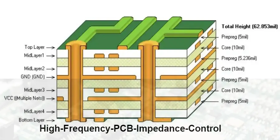
The layer stackup forms the foundation of every HF PCB design, determining signal integrity, power delivery, and electromagnetic performance. As operating frequencies exceed 10 GHz and data rates surpass 25 Gbps, stackup design becomes increasingly critical for system success. A well-optimized stackup ensures controlled impedance, minimizes crosstalk, provides effective shielding, and enables reliable manufacturing. This comprehensive guide explores the principles, methodologies, and practical considerations for designing high-performance PCB stackups that meet the demanding requirements of modern RF and high-speed digital systems.
1. The Critical Role of Stackup Design in High-frequency PCBs
Layer stackup design directly impacts every aspect of high-frequency PCB performance. Unlike low-frequency designs where stackup primarily affects routing density and cost, high-frequency applications require careful consideration of electromagnetic field distribution, signal propagation, and power delivery networks.
At frequencies above 1 GHz, the PCB stackup determines characteristic impedance tolerance, with typical targets of ±5% requiring precise control of dielectric thickness and material properties. Signal integrity depends on maintaining consistent reference planes, with interruptions causing impedance discontinuities that generate reflections exceeding acceptable limits. Crosstalk between layers increases exponentially with frequency, making proper layer assignment and shielding essential for achieving >40 dB isolation requirements.
The stackup also defines thermal management capabilities, with thermal vias and copper distribution affecting junction temperatures in high-power RF amplifiers. For multilayer PCB designs exceeding 10 layers, mechanical stability becomes critical, requiring balanced construction to prevent warpage that can cause assembly failures. Manufacturing yield directly correlates with stackup complexity, as aggressive dimensions push process capabilities and increase defect rates.
2. Material Selection Strategy for Optimal Performance
Choosing appropriate materials for each layer requires balancing electrical performance, thermal properties, mechanical stability, and cost. High-frequency designs often employ hybrid stackups combining premium RF materials with standard FR4 for non-critical layers.
High-frequency Substrate Options
For signal layers carrying frequencies above 1 GHz, low-loss materials become essential:
Rogers RO4000 Series offers excellent performance to 40 GHz:
- RO4003C: εr=3.38±0.05, Df=0.0027 at 10 GHz
- RO4350B: εr=3.48±0.05, Df=0.0037 at 10 GHz
- Temperature stable, compatible with FR4 processing
- Cost: 3-4× standard FR4
PTFE-Based Materials for ultimate performance:
- Rogers RT/duroid 5880: εr=2.20, Df=0.0009
- Taconic TLY-5: εr=2.20, Df=0.0009
- Exceptional stability, lowest loss available
- Cost: 8-10× standard FR4
Advanced Hydrocarbon Ceramics balance performance and cost:
- Isola I-Tera MT40: εr=3.45, Df=0.0031
- Panasonic Megtron 6: εr=3.61, Df=0.004
- Lead-free compatible, stable to 20 GHz
- Cost: 2-3× standard FR4
Prepreg and Core Selection
Prepreg selection critically affects impedance control and reliability:
- Match prepreg εr to core materials (±0.1 tolerance)
- Low-flow prepregs for fine features
- High Tg (>170°C) for lead-free assembly
- Controlled resin content for consistent thickness
Core materials provide mechanical stability:
- Thickness tolerance ±10% standard, ±5% for critical
- Matched CTE to prevent differential expansion
- Glass style affects εr uniformity (spread glass preferred)
3. Stackup Configuration for Different Applications
Different applications require optimized stackup configurations balancing performance requirements with manufacturing constraints.
4-Layer High-frequency Stackup
Simple designs benefit from cost-effective 4-layer configurations:
Layer 1: Signal/Components (50Ω microstrip)
    Prepreg: 0.2mm RO4450F (εr=3.52)
Layer 2: Ground Plane
    Core: 1.0mm FR4 (εr=4.4)
Layer 3: Power Plane
    Prepreg: 0.2mm RO4450F
Layer 4: Signal (50Ω microstrip)

Total thickness: 1.524mm (60 mil)
Advantages:
- Low cost, standard processing
- Good for frequencies <6 GHz
- Simple impedance control
- Adequate for many wireless applications
Limitations:
- Limited routing density
- Moderate crosstalk isolation
- Power plane resonances possible
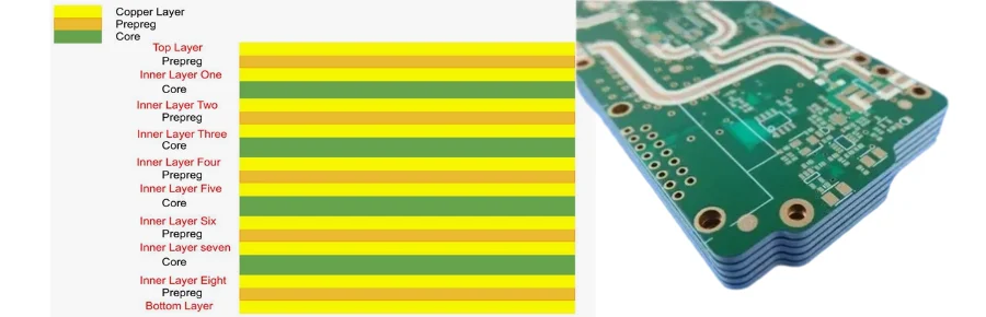
8-Layer High-Speed Digital Stackup
Complex high-speed PCB designs require more sophisticated stackups:
L1: Signal (Microstrip)
    0.1mm Prepreg
L2: Ground
    0.2mm Core
L3: Signal (Stripline)
    0.1mm Prepreg
L4: Signal (Stripline)
    0.3mm Core
L5: Power
    0.3mm Core
L6: Ground
    0.1mm Prepreg
L7: Signal (Stripline)
    0.2mm Core
L8: Signal (Microstrip)

Total: 1.6mm
Benefits:
- Multiple routing layers for density
- Excellent shielding between layers
- Distributed power/ground pairs
- Controlled impedance throughout
Advanced mmWave Stackup
Millimeter-wave applications demand specialized configurations:
L1: RF Signal (77 GHz radar)
    0.127mm RO3003 (εr=3.0)
L2: Ground
    0.254mm RO4350B
L3: Digital/Power
    0.360mm FR4
L4: Ground
    0.360mm FR4
L5: Digital
    0.254mm RO4350B
L6: Ground
    0.127mm RO3003
L7: RF Signal

Total: 1.524mm
Features:
- Ultra-low loss materials for RF layers
- Hybrid construction for cost optimization
- Symmetric build prevents warpage
- Via backdrill zones defined
4. Impedance Planning and Control in Stackup Design
Achieving consistent impedance across all signal layers requires careful planning during stackup design. Each transmission line type—microstrip, stripline, and coplanar waveguide—has unique requirements that must be accommodated.
Microstrip Impedance Optimization
Microstrip on outer layers provides easy component access but requires careful control:
Target: 50Ω ±5%
- Calculate trace width based on dielectric height
- Account for solder mask effect (+2-3Ω)
- Consider copper roughness at high frequencies
- Plan for etch factor compensation
Example calculation for RO4003C:
- Dielectric height: 0.203mm (8 mil)
- Trace width: 0.432mm (17 mil)
- Achieved impedance: 50.2Ω
Stripline Configuration
Stripline offers superior shielding and consistent impedance:
Benefits:
- No frequency dispersion
- Better crosstalk isolation (>6dB improvement)
- Protected from external interference
- Consistent εr (no air interface)
Design considerations:
- Center traces between planes for symmetry
- Maintain 2:1 height-to-width ratio minimum
- Account for glass weave effects
- Plan via transitions carefully
Differential Pair Implementation
High-speed differential signals require special attention:
- Edge-coupled vs. broadside-coupled routing
- Target 100Ω differential (50Ω odd-mode)
- Maintain coupling through layer transitions
- Match propagation delay within pairs
5. Power and Ground Plane Strategy
Effective power distribution and grounding are essential for high-frequency performance. The stackup must provide low-impedance power delivery while maintaining signal integrity.
Power/Ground Plane Pairing
Adjacent power and ground planes create distributed capacitance:
Capacitance calculation: C = ε₀ × εr × A / d
For 100mm × 100mm planes with 0.1mm spacing: C = 8.85 × 4.4 × 10,000 / 0.1 = 3.9nF
This provides high-frequency decoupling, reducing power supply noise and improving signal integrity.
Plane Assignment Strategy
Optimize plane placement for different frequencies:
Digital sections: Tight power/ground coupling
- 0.1mm spacing for >1 GHz operation
- Multiple voltage domains on single layer
- Split planes with bridge capacitors
RF sections: Continuous ground planes
- No splits under RF traces
- Guard rings for isolation
- Via fencing at board edges
Mixed-signal: Separate analog/digital grounds
- Star point connection
- Ferrite beads for HF isolation
- Careful routing across splits
EMI Control Through Stackup
Proper stackup design significantly reduces electromagnetic emissions:
- Bury high-speed signals between planes
- Implement 20-H rule for plane dimensions
- Add stitching vias at λ/20 intervals
- Use edge plating for improved shielding
6. Why Choose HILPCB for High-frequency PCB Stackup Design
HILPCB provides comprehensive stackup design and manufacturing services optimized for high-frequency applications:
- Expert Consultation: RF and signal integrity engineers review your requirements
- Material Inventory: Complete range of high-frequency laminates in stock
- Simulation Services: Pre-build modeling and impedance prediction
- Manufacturing Capability: 2-40 layers with ±3% impedance control
- Validation Testing: TDR, cross-section, and reliability testing
- Quick Turnaround: 24-hour stackup proposals, 5-day prototypes
Our experience spans:
- 5G infrastructure and small cells
- Automotive radar (24/77 GHz)
- High-speed computing (56 Gbps+)
- Aerospace and defense systems
- Test and measurement equipment
7. Frequently Asked Questions (FAQ)
Q1: How many layers do I need for my high-frequency design?
A: Depends on circuit complexity and frequency. Simple RF circuits work with 4 layers below 6 GHz. Complex digital+RF systems typically need 8-12 layers. Above 20 GHz, consider 6+ layers for proper shielding and routing.
Q2: Should I use the same material throughout the stackup?
A: Not necessarily. Hybrid stackups using RF materials only where needed (typically outer layers and critical signal layers) can reduce cost by 40-60% while maintaining performance. Ensure CTE matching to prevent reliability issues.
Q3: How does stackup affect impedance tolerance?
A: Stackup directly determines impedance through dielectric thickness and εr. Thinner dielectrics give tighter impedance control but require finer trace widths. Target ±10% thickness tolerance for ±5% impedance control.
Q4: What's the impact of asymmetric stackups?
A: Asymmetric stackups cause warpage during assembly, potentially exceeding 0.75% bow/twist limits. They also create uneven stress distribution. Always use symmetric stackups unless absolutely necessary, then implement compensation strategies.
Q5: How do I minimize crosstalk between layers?
A: Route perpendicular on adjacent signal layers, maintain ground planes between signal layers, use thinner dielectrics for tighter coupling to reference planes, and implement proper via shielding. Target >35dB isolation for sensitive signals.
Q6: When should I use sequential lamination?
A: Sequential lamination is necessary for HDI PCB with stacked or staggered vias, building up from a core to create complex via structures. It's essential for high-density designs but adds 20-30% to manufacturing cost.
Ready to Optimize Your PCB Stackup?
Our engineering team specializes in designing high-performance stackups for demanding RF and high-speed applications. Get expert consultation on your next project.