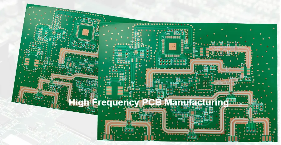
The manufacturing of high-frequency PCBs for RF and microwave applications demands exceptional precision, specialized equipment, and rigorous process control that far exceeds standard PCB fabrication requirements. With operating frequencies extending from 1 GHz to beyond 100 GHz in modern 5G and radar systems, every aspect of the manufacturing process—from material handling to final inspection—directly impacts electrical performance and signal integrity.
Professional RF PCB manufacturers must maintain impedance tolerances within ±3%, achieve dielectric losses below 0.002, and control dimensional accuracy to ±25μm while processing challenging materials like PTFE composites and ceramic-filled substrates. This comprehensive guide explores the advanced manufacturing techniques, specialized equipment, and quality systems essential for producing high-performance RF/microwave PCBs that meet the stringent requirements of aerospace, defense, telecommunications, and automotive radar applications.
Understanding PTFE and High-frequency Material Processing Challenges
The foundation of successful high-frequency PCB manufacturing lies in understanding the unique properties and processing requirements of RF substrate materials. Unlike conventional FR4, PTFE-based materials exhibit low surface energy, high thermal expansion coefficients, and soft mechanical properties that demand fundamentally different processing approaches.
Material Behavior During Processing
PTFE substrates undergo significant dimensional changes during thermal cycling, with CTE values 3-4 times higher than FR4 in the Z-axis. This characteristic requires modified lamination cycles with reduced pressure (50-150 PSI vs. 200-400 PSI for FR4), controlled temperature ramps not exceeding 3°C/minute, extended cool-down periods to prevent stress-induced warpage, and specialized tooling to accommodate material movement.
Critical Processing Windows
| Material Type | Peak Temperature | Pressure Range | Dwell Time | Cool Rate |
|---|---|---|---|---|
| PTFE Woven Glass | 240-280°C | 50-100 PSI | 60-90 min | <3°C/min |
| Ceramic PTFE | 260-300°C | 100-150 PSI | 45-75 min | <5°C/min |
| Hydrocarbon | 180-220°C | 150-250 PSI | 30-60 min | <8°C/min |
| LCP | 280-320°C | 200-300 PSI | 90-120 min | <2°C/min |
Manufacturing facilities must maintain precise environmental controls with temperature at 20±2°C and relative humidity below 50% to prevent moisture absorption that can cause delamination during high-temperature processing.
Advanced Lamination Technologies for RF Substrates
Fusion Bonding Systems for PTFE Materials
Modern fusion bonding technology eliminates traditional adhesive prepregs, achieving superior electrical performance through direct PTFE-to-PTFE molecular bonding. This revolutionary process has transformed how manufacturers approach multilayer PCB construction for demanding RF applications.
Equipment Specifications and Requirements:
- Vacuum-assisted hydraulic presses with ±1°C temperature uniformity
- Real-time pressure profiling with 16+ independent zones
- Nitrogen atmosphere capability for oxidation prevention
- Automated data logging for process validation
The fusion bonding cycle consists of four critical phases that must be precisely controlled. During the vacuum application phase (0-30 minutes), the system achieves -28 to -29.5" Hg vacuum level while ramping temperature from ambient to 150°C, eliminating voids and removing moisture. The molecular activation phase (30-90 minutes) increases temperature to 280-320°C depending on material specifications, with gradual pressure ramping to 100 PSI under nitrogen atmosphere. The bonding phase (90-150 minutes) maintains stable temperature within ±2°C and pressure within ±5 PSI while molecular chain interdiffusion occurs. Finally, the controlled cooling phase (150-240 minutes) reduces temperature at 2-3°C/minute maximum with staged pressure release, ensuring the panel reaches below 50°C before removal.
Sequential Lamination for Complex Multilayers
Complex multilayer structures require sequential build-up processes to maintain layer-to-layer registration and prevent material degradation. Consider an 8-layer RF board construction:
Step 1: Core Preparation (Layers 3-6) The process begins with RO4003C material at 0.508mm thickness, using standard lamination parameters to achieve ±25μm registration accuracy. This forms the stable foundation for subsequent layers.
Step 2: Sequential Addition (Layers 2,7) RO4450F prepreg bonds the next layers at reduced temperature (220°C maximum) to prevent core material degradation. CCD camera systems maintain precise alignment throughout the process.
Step 3: Outer Layer Lamination (Layers 1,8) Final lamination adds 1/2 oz copper foil, achieving total thickness of 2.36mm ±0.05mm with impedance verification confirming 50Ω ±2Ω tolerance.
Precision Drilling and Hole Formation Technologies
Laser Drilling Systems for Microvias
High-frequency applications increasingly utilize HDI PCB technology with laser-drilled microvias for improved signal integrity. The implementation of UV laser systems has revolutionized microvia formation in RF substrates.
UV Laser System Parameters: Modern systems employ 355nm wavelength (frequency-tripled Nd:YAG) lasers with 15-25 nanosecond pulse duration, delivering 0.1-2.0 mJ adjustable pulse energy. Beam quality maintains M² < 1.3 with positioning accuracy of ±10μm, essential for precise via placement in dense RF circuits.
Material-Specific Drilling Optimization:
For PTFE-based materials: Power density ranges from 5-8 J/cm² with pulse frequency of 10-20 kHz. The spiral drilling pattern ensures clean sidewalls, while post-drill cleaning uses plasma only, avoiding chemical desmear that could damage the substrate.
For ceramic-filled substrates: Higher power density of 10-15 J/cm² compensates for material hardness, with reduced pulse frequency of 5-10 kHz preventing excessive heat buildup. Multiple pass strategies with debris removal between passes ensure consistent hole quality.
Controlled Depth Drilling and Backdrilling Excellence
Backdrilling eliminates via stubs that cause resonances at high frequencies, requiring exceptional depth control accuracy. Modern CNC systems integrate multiple sensing technologies to achieve unprecedented precision.
Advanced Depth Control Implementation:
The system employs optical encoders with 0.1μm resolution, acoustic emission monitoring for breakthrough detection, automatic tool length compensation, and real-time force feedback control. This multi-sensor approach ensures consistent depth accuracy across thousands of holes.
Stub Length Requirements by Frequency:
- Above 20 GHz: Maximum 0.25mm stub length
- 10-20 GHz: Maximum 0.50mm stub length
- 5-10 GHz: Maximum 1.00mm stub length
- Below 5 GHz: Maximum 2.00mm stub length
Process validation involves cross-sectional analysis of 5% of backdrilled vias, with 100% inline measurement using laser depth gauging systems achieving ±10μm accuracy.
Metallization Processes for High-frequency Materials
Revolutionary Surface Treatment Technologies
The low surface energy of PTFE materials (18-20 dyne/cm) requires aggressive surface modification to achieve reliable copper adhesion. Recent advances in atmospheric plasma technology offer significant advantages over traditional sodium etching.
Atmospheric Plasma Treatment Systems:
Modern plasma systems operate with carefully controlled gas compositions of Argon/Oxygen/Nitrogen mixtures, delivering 100-200 W/cm² power density at treatment speeds of 0.5-2.0 m/minute. This process increases surface energy to >45 dyne/cm without the environmental hazards of wet chemistry.
Quality verification employs multiple analytical techniques:
- Contact angle measurement requiring <30° for adequate wetting
- Dyne ink testing confirming >42 dyne/cm surface energy
- XPS analysis verifying surface chemistry modifications
- AFM measurement ensuring Ra 0.5-1.0μm surface roughness
Direct Metallization: The Future of Copper Deposition
Emerging conductive polymer technologies eliminate traditional electroless copper, offering superior performance for high-frequency applications.
The Three-Stage Direct Metallization Process:
Conditioning Stage (2-3 minutes): Mild alkaline solution modifies surface charge at 40-45°C, preparing the substrate for polymer adhesion.
Polymer Deposition (3-5 minutes): Conductive polymer forms a 40-60nm layer with sheet resistance <1000 Ω/square, providing the conductive seed layer for subsequent plating.
Electroplating (Immediate): Direct copper plating begins at 1-2 ASF, ramping to 20 ASF over 10 minutes for optimal grain structure.
This technology eliminates magnetic particles that can affect high-frequency performance, provides uniform coverage in high aspect ratio vias, reduces processing time by 40%, and meets stringent environmental regulations.
Controlled Impedance Manufacturing Excellence
Real-time Impedance Monitoring and Control
Modern manufacturing incorporates inline impedance measurement systems that provide immediate process feedback, enabling real-time adjustments to maintain specifications.
Automated Test System Architecture:
The system integrates TDR units with 35ps rise time and 0.1Ω resolution, robotic probe stations achieving ±12μm positioning accuracy, comprehensive database systems for SPC charting, and feedback algorithms for automatic process adjustment.
Process Flow with Inline Testing:
Each panel enters the test station where barcode scanning identifies the specific design. The database queries appropriate test parameters, loading the corresponding program. Automated probes contact designated test points, performing TDR measurements within seconds. Results immediately update control charts, triggering process adjustments if measurements approach control limits.
Intelligent Process Compensation
Sophisticated algorithms predict and compensate for process variations, ensuring consistent impedance across production runs.
Etch Factor Compensation Example:
For a target trace width of 0.381mm (15 mil) with measured etch factor of 2.5:1 and 35μm copper thickness:
- Base width: 0.381mm
- Etch compensation: 2 × 35μm × 0.8 = 0.056mm
- Artwork adjustment: 0.381 + 0.056 = 0.437mm
- Final achieved width: 0.381mm ±0.025mm
The system maintains a historical database of over 10,000 measurements, employing machine learning to predict optimal compensation values based on current chemistry conditions, copper thickness, and substrate characteristics.
Quality Assurance Through Advanced Metrology
3D Automated Optical Inspection Revolution
Latest generation AOI systems provide comprehensive dimensional verification with unprecedented accuracy:
System Capabilities:
- Resolution: 0.5μm in X/Y axes, 0.1μm in Z axis
- Field of view: 50mm × 50mm per capture
- Measurement speed: 100 cm²/second throughput
- Data density: >10 million measurement points per panel
These systems measure trace width/spacing with ±1μm accuracy, perform non-contact copper thickness measurement, detect solder mask registration within ±5μm, and calculate surface roughness parameters (Ra, Rz) for signal integrity analysis.
Comprehensive Electrical Testing Protocols
Network Analyzer Integration for RF Verification:
Production testing extends beyond traditional continuity and isolation checks to include full S-parameter characterization:
- Frequency range: 10 MHz to 40 GHz coverage
- Calibration: SOLT methodology with verification standards
- Test structures: Dedicated coupons for loss and impedance
- Data analysis: Automatic pass/fail determination with detailed reporting
Environmental Stress Testing:
Qualification protocols verify performance under extreme conditions:
- Thermal cycling: -55°C to +125°C, 500 cycles minimum
- Humidity resistance: 85°C/85% RH for 1000 hours
- Thermal shock: 288°C solder float for 10 seconds
- Vibration testing: MIL-STD-810G compliance
Manufacturing Excellence for Specialized Applications
5G Infrastructure Requirements
Manufacturing 5G PCBs demands exceptional precision for both sub-6 GHz and mmWave frequency bands:
Sub-6 GHz Specifications:
- Impedance control: ±3% tolerance
- Loss tangent: <0.005 at operating frequency
- Via stub length: <1mm maximum
- Layer-to-layer registration: ±50μm
mmWave Band Challenges (24-40 GHz):
- Surface roughness: <1μm Rz
- Impedance control: ±2% tolerance
- Via stub elimination: mandatory backdrilling
- Copper thickness uniformity: ±10% maximum variation
Automotive Radar Manufacturing
77 GHz automotive radar systems present unique manufacturing challenges:
Critical Requirements:
- Material stability: -40°C to +150°C operation
- Vibration resistance: IATF 16949 compliance
- Long-term reliability: 15-year service life
- Cost optimization: High-volume production capability
Manufacturing processes must accommodate these requirements while maintaining electrical performance specifications tighter than traditional RF applications.
Environmental Compliance and Sustainability
Green Manufacturing Initiatives
Modern high-frequency PCB manufacturing increasingly emphasizes environmental responsibility:
Waste Reduction Strategies:
- Closed-loop water recycling: 95% water reuse
- Copper recovery: Electrowinning from etch solutions
- PTFE recycling: Thermal depolymerization and reuse
- Energy optimization: Heat recovery from lamination presses
Chemical Management:
- Lead-free HASL implementation for RoHS compliance
- Elimination of PFOS/PFOA compounds
- Reduced chemistry consumption through process optimization
- Zero-discharge goals for hazardous materials
Why Choose HILPCB for High-frequency PCB Manufacturing
HILPCB combines decades of RF manufacturing expertise with state-of-the-art equipment and comprehensive quality systems:
Manufacturing Capabilities:
- PTFE processing with specialized lamination equipment
- Laser drilling for HDI microvia technology
- Controlled impedance with ±3% tolerance
- Backdrilling with ±25μm depth accuracy
- Sequential lamination for complex multilayers
Quality Certifications:
- ISO 9001:2015 quality management
- IPC-A-600 Class 3 workmanship
- AS9100D aerospace qualification
- IATF 16949 automotive certification
Technical Support:
- DFM analysis and optimization
- Material selection guidance
- Stackup design assistance
- Impedance modeling and prediction