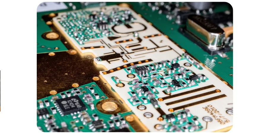
The selection of appropriate packaging for high-frequency PCBs critically impacts signal integrity, thermal performance, and overall system reliability. As frequencies extend beyond 77 GHz and integration density increases, packaging technology has evolved from simple wire-bonded solutions to sophisticated 3D architectures. Modern HF PCB packaging must minimize parasitic effects, manage heat dissipation, and provide electromagnetic shielding while maintaining manufacturability and cost-effectiveness.
Our comprehensive packaging solutions span from traditional surface-mount technologies to cutting-edge system-in-package implementations, enabling optimal performance across telecommunications, automotive radar, and aerospace applications.
Understanding Package Selection for High-frequency Applications
Package selection for high-frequency circuits requires balancing electrical performance, thermal management, mechanical reliability, and cost. Each packaging type offers distinct advantages and trade-offs that must be carefully evaluated against application requirements.
1. Electrical Performance Considerations
At high frequencies, package parasitics dominate circuit behavior. Bond wire inductance, lead frame capacitance, and package resonances can destroy signal integrity if not properly managed. Modern packaging solutions minimize these effects through shortened interconnects, controlled impedance transitions, and optimized ground structures. For high-speed PCB applications exceeding 10 Gbps, we evaluate packages based on insertion loss, return loss, and crosstalk specifications across the operating bandwidth.
2. Thermal Management Requirements
High-frequency circuits often dissipate significant power in compact spaces. Package thermal resistance determines maximum operating power and reliability. We consider junction-to-ambient thermal paths, incorporating features like exposed pads, thermal vias, and integrated heat spreaders. For power amplifier applications, packages with thermal resistance below 10°C/W enable reliable operation at full rated power.
3. Manufacturing and Assembly Compatibility
Package selection impacts assembly yield, rework capability, and overall production cost. While chip-scale packages offer superior electrical performance, they require advanced assembly equipment and tighter process controls. We balance performance requirements with manufacturing capabilities, ensuring reliable production scaling from prototypes to volume.
4. Environmental and Reliability Factors
Operating environment dictates package construction and materials. Automotive applications require AEC-Q100 qualification with extended temperature ranges. Aerospace demands hermetic sealing for altitude operation. We select packages meeting specific environmental requirements while maintaining RF performance across conditions.
Ball Grid Array (BGA) Packages for High-frequency Design
BGA packages have become the workhorse of high-frequency digital and mixed-signal applications, offering high pin counts with manageable parasitics. The array configuration provides short, controlled interconnects ideal for maintaining signal integrity.
Advanced BGA Implementations
Modern BGA packages incorporate sophisticated features optimizing high-frequency performance. Low-loss organic substrates with controlled dielectric constant maintain impedance from die to PCB. Multiple ground planes within the package substrate provide shielding and controlled impedance environments. Via-in-pad technology eliminates stub effects, critical for signals above 5 GHz.
Our BGA packaging solutions include:
- Fine-Pitch BGA (FBGA) with 0.5mm-0.8mm pitch for high-density applications
- Thermally Enhanced BGA incorporating copper slugs for >10W dissipation
- Cavity BGA for reduced loop inductance in RF front-ends
- Molded Array Process BGA (MAPBGA) for cost-sensitive consumer products
- High-Temperature Co-fired Ceramic (HTCC) BGA for extreme environments
For HDI PCB designs, we implement microvia-in-pad structures directly under BGA balls, eliminating via stubs while maintaining routability. This approach is essential for differential pairs operating above 10 Gbps, where via stubs create impedance discontinuities and signal degradation.
BGA Design Guidelines for RF Performance
Successful BGA implementation requires careful attention to PCB design details. Signal ball assignments should minimize layer transitions, with critical high-speed signals routed on outer layers. Ground balls should surround high-frequency signals, providing coaxial-like shielding. Power delivery requires distributed decoupling capacitors placed as close as possible to power balls.
Thermal management in BGA packages utilizes thermal balls connected to internal copper planes. We typically allocate 20-30% of ball count for thermal management in high-power applications. Via arrays under the package conduct heat to internal layers or bottom-side heatsinks.
Quad Flat No-Lead (QFN) Packages for Compact RF Solutions
QFN packages offer excellent RF performance in minimal footprint, making them ideal for space-constrained wireless applications. The leadless design minimizes parasitic inductance while the exposed pad provides superior thermal and electrical grounding.
QFN Advantages for High-frequency Circuits
The near-chip-scale dimensions of QFN packages reduce interconnect lengths to under 1mm, minimizing transmission line effects. Wire bond inductance typically measures 1-2 nH, significantly lower than leaded packages. The exposed pad creates a low-inductance ground connection, essential for stable amplifier operation and effective bypassing.
QFN variants optimized for RF applications include:
- Air-Cavity QFN eliminating mold compound losses above 20 GHz
- Flip-Chip QFN using bumped die for minimal interconnect parasitics
- Multi-Row QFN providing higher pin counts for complex RF SoCs
- Wettable Flank QFN enabling optical inspection for high-reliability applications
Manufacturing Considerations for QFN Assembly
QFN assembly requires precise process control for reliable solder joints. The lack of leads eliminates self-alignment, demanding accurate placement and solder paste printing. We implement:
- Solder paste aperture reduction (80-90% of pad size) preventing bridging
- Optimized reflow profiles minimizing voiding under exposed pads
- X-ray inspection verifying solder joint formation and void content
- Underfill application for high-vibration environments
For rigid-flex PCB applications, QFN packages mount on rigid sections with careful attention to stress relief at flex transitions.
Chip-on-Board (COB) Technology for Ultimate Performance
COB technology eliminates package parasitics entirely by mounting bare die directly on the PCB substrate. This approach provides the shortest possible interconnects and highest frequency performance achievable in PCB-based systems.
Direct Die Attach Methods
Wire Bonding remains the most common COB interconnect method, suitable for frequencies up to 40 GHz with proper design. Gold or aluminum wires, typically 25μm diameter, connect die pads to PCB traces. Multiple parallel bonds reduce inductance for power and ground connections. Wedge bonding provides lower loop height than ball bonding, critical for maintaining controlled impedance.
Flip-Chip Bonding offers superior high-frequency performance through direct bump connections. Solder bumps, copper pillars, or gold stud bumps provide interconnects under 100μm long. This technique enables operation beyond 100 GHz with proper design. Underfill encapsulation provides mechanical support and environmental protection.
COB Implementation Challenges and Solutions
COB assembly requires specialized equipment and processes:
- Die attach using conductive or non-conductive adhesives
- Wire bonding with programmable ultrasonic bonders
- Plasma cleaning for reliable wire bond adhesion
- Glob-top or dam-and-fill encapsulation for protection
Thermal management becomes critical with heat concentrated in small die areas. We implement:
- High thermal conductivity substrates (aluminum nitride, copper-invar-copper)
- Thermal vias arrays under die attach areas
- Direct liquid cooling for high-power applications
System-in-Package (SiP) and 3D Integration
SiP technology integrates multiple die, passives, and interconnects within a single package, creating complete functional systems. This approach optimizes performance while reducing PCB complexity and size.
Advanced SiP Architectures
Modern SiP implementations leverage multiple technologies for optimal integration:
Package-on-Package (PoP) stacks memory over logic, minimizing interconnect length for high-bandwidth interfaces. Through-mold vias (TMV) provide vertical connections without wire bonds.
Embedded Die Packaging places thinned die within PCB substrate layers, eliminating wire bonds entirely. This approach enables integration of RF front-ends with minimal parasitics.
Fan-Out Wafer Level Packaging (FOWLP) redistributes die I/O over larger area, relaxing PCB design rules while maintaining excellent electrical performance.
Integration Benefits for RF Systems
SiP technology enables complete RF subsystems including:
- Integrated passive devices (IPD) for filters and matching networks
- Multiple die for transceiver, PA, and LNA functions
- Embedded antennas for complete wireless solutions
- Shielding structures for isolation between blocks
This integration reduces size by 50-70% compared to discrete implementations while improving performance through shortened interconnects and optimized impedance matching.
Package Selection Guidelines for Specific Applications
Choosing optimal packaging requires matching technology capabilities with application requirements. We provide comprehensive consultation ensuring appropriate selection for your specific needs.
5G and Wireless Infrastructure
5G base stations demand packages supporting massive MIMO arrays with hundreds of RF channels. Key requirements include:
- Low-loss transitions for 28/39 GHz operation
- Thermal management for continuous operation
- High integration for size/weight reduction
- Cost optimization for commercial deployment
Recommended solutions: Air-cavity BGA for front-ends, FOWLP for transceivers, SiP for complete RF chains.
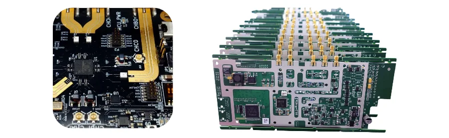
Automotive Radar Systems
77 GHz automotive radar requires robust packaging surviving harsh environments:
- -40°C to +150°C operation
- Vibration resistance to 50G
- Moisture resistance (MSL 1)
- Long-term reliability (15 years)
Optimal packages: Cavity QFN for transceivers, COB for maximum performance, hermetic ceramic for extreme conditions.
Test and Measurement Equipment
High-performance instruments demand ultimate signal fidelity:
- Minimal phase noise and jitter
- Bandwidth beyond 70 GHz
- Superior isolation between channels
- Calibration stability
Preferred approaches: COB with controlled impedance substrates, custom ceramics for critical paths, modular SiP for flexibility.
High-frequency PCB Packaging and Assembly Solutions
At HILPCB, we provide comprehensive packaging solutions, taking your design from prototype to full-scale production with exceptional precision for demanding high-frequency applications. Our state-of-the-art Class 10,000 cleanroom facilities ensure the integrity of your designs, offering precise die attach and wire bonding while preventing contamination that could affect performance. Automated equipment delivers placement accuracy of ±12μm, which is essential for fine-pitch packages. Additionally, we conduct environmental stress screening to validate the reliability of your PCB across various temperature, humidity, and mechanical conditions.
Our turnkey assembly services combine packaging with PCB manufacturing, delivering a complete solution from bare boards to fully tested systems. This integration guarantees that key factors such as impedance matching, thermal management, and signal integrity are optimized throughout the entire signal chain, ensuring high performance from start to finish.
We adhere to rigorous quality standards, certified to ISO 9001, IPC-A-610, and J-STD-001, ensuring consistent, reliable production. By using statistical process control to monitor critical parameters and maintaining a Cpk >1.33, we ensure top-tier production quality. Our system also provides full traceability from raw materials to final shipment, allowing us to quickly resolve any challenges that arise during the production process.