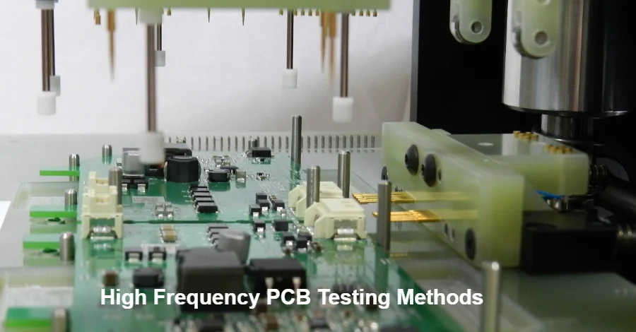
Testing high-frequency PCBs requires specialized equipment, methodologies, and expertise that go far beyond traditional DC continuity checks. As operating frequencies push beyond 40 GHz and data rates exceed 56 Gbps, comprehensive testing becomes critical for ensuring product performance and reliability. At the heart of every successful high-frequency PCB lies a rigorous testing strategy that validates signal integrity, impedance control, and electromagnetic performance.
Our advanced testing capabilities enable manufacturers to verify PCB performance from prototype through production, ensuring every board meets stringent specifications for 5G infrastructure, automotive radar, and aerospace applications.
Essential High-frequency PCB Testing Equipment and Setup
The foundation of accurate high-frequency testing lies in properly calibrated equipment and controlled test environments. Modern RF and microwave testing demands instruments capable of measurements from DC to millimeter-wave frequencies with exceptional accuracy and repeatability.
1. Time Domain Reflectometry (TDR) Systems
TDR testing provides critical insight into impedance variations along transmission lines. Our TDR systems feature 35-picosecond rise times enabling accurate characterization up to 20 GHz equivalent bandwidth. The spatial resolution of 1mm allows precise location of impedance discontinuities, while ±0.5Ω impedance accuracy ensures reliable pass/fail determination. For high-speed PCB applications, we employ differential TDR capable of measuring both odd and even mode impedances simultaneously.
2. Vector Network Analyzers (VNA)
VNA testing forms the backbone of S-parameter characterization for frequencies from 10 MHz to 110 GHz. Our calibrated VNA systems provide insertion loss measurement accuracy of ±0.1 dB and return loss measurements exceeding 40 dB dynamic range. Multi-port VNAs enable complete characterization of differential structures, crosstalk evaluation, and mode conversion analysis critical for high-speed serial links.
3. Real-Time Oscilloscopes
Eye diagram analysis requires oscilloscopes with bandwidth exceeding 2.5 times the fundamental frequency. Our 70 GHz real-time oscilloscopes capture millions of waveforms for comprehensive jitter analysis, providing RJ/DJ separation, eye height/width measurements, and BER extrapolation. Advanced triggering capabilities enable isolation of specific data patterns for detailed signal integrity analysis.
4. Spectrum Analyzers and EMI Receivers
Electromagnetic compatibility testing utilizes spectrum analyzers covering 9 kHz to 40 GHz with phase noise better than -110 dBc/Hz at 10 kHz offset. Near-field probe sets enable precise location of emissions sources, while our 3-meter semi-anechoic chamber provides pre-compliance testing to CISPR and FCC standards.
5. Environmental Test Chambers
Reliability validation requires testing across temperature extremes and humidity conditions. Our environmental chambers provide -65°C to +200°C temperature range with ±0.5°C stability, humidity control from 10% to 98% RH, and combined temperature/humidity/vibration testing for comprehensive environmental stress screening.
Impedance and Signal Integrity Testing Protocols
Maintaining controlled impedance is fundamental to high-frequency PCB performance. Our comprehensive testing protocols ensure every board meets specified impedance tolerances while validating overall signal integrity.
TDR Testing Best Practices
Effective TDR testing requires careful attention to launch conditions, calibration, and interpretation. We begin with proper calibration using precision air lines and short/open/load standards. Test fixtures employ controlled impedance launches matched to the device under test, minimizing measurement artifacts.
Our standard TDR test procedure includes:
- Pre-test Verification using known impedance standards to confirm system calibration
- Multiple Measurement Points across the panel to capture process variations
- Temperature Stabilization allowing boards to reach ambient temperature before testing
- Automated Data Collection with statistical analysis for process control
- Correlation Studies comparing TDR results with VNA measurements for validation
- Documentation Package including impedance profiles, statistics, and pass/fail determination
For multilayer PCB designs, we test representative traces on each signal layer, capturing both microstrip and stripline configurations. Differential impedance testing employs true differential TDR with matched launches, ensuring accurate characterization of coupled structures.
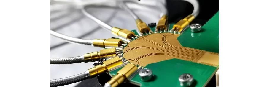
S-Parameter Measurements and Analysis
S-parameter testing provides frequency-domain characterization essential for validating high-frequency performance. Our methodology ensures accurate, repeatable measurements correlated with simulation predictions.
The measurement process encompasses:
- SOLT (Short-Open-Load-Thru) calibration to the measurement plane
- De-embedding of test fixtures using time-domain gating or TRL calibration
- Temperature-controlled measurements for thermal coefficient characterization
- Mixed-mode S-parameter conversion for differential structures
- Causality verification ensuring physical measurement validity
- Extraction of RLGC parameters for circuit simulation models
Critical parameters monitored include insertion loss (S21), return loss (S11), and crosstalk (S31/S41) across the operating frequency range. For high-speed digital applications, we extract eye diagrams from S-parameter data, predicting system-level performance before assembly.
Production Testing Strategies for High-Volume Manufacturing
Transitioning from prototype validation to production testing requires balancing thoroughness with throughput. Our production test strategies ensure quality while maintaining cost-effectiveness.
In-Line Testing Implementation
Modern PCB manufacturing integrates testing throughout the production process rather than relying solely on final inspection. This approach identifies issues early, reducing scrap costs and improving yields.
Automated Optical Inspection (AOI) systems inspect every panel after etching, checking trace width, spacing, and registration. Advanced 3D AOI provides solder paste volume measurements critical for SMT assembly of fine-pitch components. Machine learning algorithms reduce false calls while ensuring defect detection rates exceeding 99.9%.
Flying Probe Testing provides electrical verification without requiring bed-of-nails fixtures. Our systems test impedance, continuity, and isolation at speeds up to 60 measurements per second. Boundary scan integration enables testing of complex digital circuits without physical access to all nodes.
In-Circuit Testing (ICT) validates component placement and values after assembly. Combined with functional testing, ICT ensures both manufacturing quality and circuit operation before shipment.
Statistical Process Control and Yield Management
Maintaining consistent quality in high-volume production requires robust statistical process control. We monitor key parameters including impedance, insertion loss, and layer registration, using control charts to identify trends before they impact yield.
Our SPC implementation includes:
- Real-time data collection from all test stations
- Automated alert generation for out-of-control conditions
- Cpk analysis ensuring process capability exceeds 1.33
- Correlation analysis identifying root causes of variation
- Predictive maintenance based on equipment performance trends
This data-driven approach has enabled us to achieve:
- First-pass yields exceeding 98% for standard designs
- Impedance control within ±3% for 95% of production
- Defect rates below 50 PPM for critical parameters
Specialized Testing for mmWave Applications
Testing PCBs operating above 20 GHz presents unique challenges requiring specialized techniques and equipment. Surface roughness, dielectric anisotropy, and conductor losses become dominant factors affecting performance.
Over-the-Air (OTA) Testing
Many mmWave applications integrate antennas directly on the PCB, necessitating OTA testing for complete validation. Our compact antenna test range provides:
- Frequency coverage to 90 GHz
- Pattern measurement accuracy ±0.5 dB
- Polarization purity better than -30 dB
- Temperature-controlled testing for thermal characterization
We measure critical antenna parameters including gain, efficiency, beamwidth, and sidelobe levels. For phased array applications, we verify beam steering accuracy and element-to-element phase matching.
Material Characterization at Microwave Frequencies
Accurate material properties are essential for successful mmWave design. We employ multiple techniques for comprehensive characterization:
Split-Post Dielectric Resonator (SPDR) measurements provide precise dielectric constant and loss tangent from 1-20 GHz. The resonant technique achieves Dk accuracy of ±0.5% and Df resolution of 0.0001.
Free-Space Methods extend measurements to 110 GHz using focused beam systems. Non-contact measurement eliminates fixture effects while accommodating large panel sizes.
Stripline Resonator Tests validate material properties in actual PCB constructions, capturing effects of copper roughness and processing variations.
Environmental and Reliability Testing
High-frequency PCBs must maintain performance across environmental extremes. Our comprehensive reliability testing validates long-term stability and durability.
Thermal Cycling and Shock Testing
Temperature extremes stress materials and interconnections, potentially causing failures. Our testing protocols follow IPC and military standards:
- Temperature range: -65°C to +150°C
- Ramp rates: 10-15°C/minute
- Dwell time: 10-30 minutes at extremes
- Cycle count: 100-1000 depending on application
We monitor resistance changes during cycling, identifying potential failure sites before catastrophic failure. Cross-sectioning after testing reveals microstructural changes invisible to external inspection.
Moisture Resistance and HAST Testing
Humidity degrades high-frequency performance through moisture absorption and corrosion. Our testing includes:
85/85 Testing: 85°C and 85% relative humidity for 1000 hours simulates years of field exposure. We measure impedance and loss changes, correlating with moisture uptake.
HAST (Highly Accelerated Stress Testing): Elevated temperature and pressure accelerate moisture penetration, revealing weaknesses in days rather than months.
Moisture Sensitivity Level (MSL) classification ensures proper handling during assembly, preventing popcorning and delamination during reflow.
Customized Testing Solutions for Specific Applications
Different applications require tailored testing approaches optimized for their unique requirements. We develop custom test solutions addressing specific industry needs.
5G Infrastructure Testing
5G base stations demand exceptional performance across multiple frequency bands. Our 5G-specific testing includes:
- Massive MIMO antenna array validation
- Beamforming accuracy verification
- Power amplifier linearity testing
- Thermal performance under full power
- Passive intermodulation (PIM) testing below -150 dBc
We simulate real-world conditions including temperature variation, vibration, and multi-carrier operation, ensuring reliable field performance.
Automotive Radar Validation
77 GHz automotive radar requires stringent testing for safety-critical applications:
- Phase noise measurement below -90 dBc/Hz at 1 kHz
- Range resolution testing using delay lines
- Doppler accuracy verification
- Environmental stress screening per AEC-Q100
- EMC testing to CISPR 25 Class 5
Our automotive-qualified facility meets IATF 16949 requirements, providing full traceability and documentation for Tier 1 suppliers.
Aerospace and Defense Requirements
Military and aerospace applications demand the highest reliability levels. Our testing capabilities include:
- Shock and vibration per MIL-STD-810
- Altitude simulation to 100,000 feet
- Salt fog exposure testing
- Thermal vacuum compatibility
- Radiation tolerance screening
We maintain AS9100D certification and comply with ITAR regulations for controlled technology.
Advantages of Choosing HILPCB for High-frequency PCB Manufacturing and Testing
At HILPCB, we understand the importance of precision and reliability in HF PCB design and testing. Whether you’re developing advanced RF and microwave circuits for 5G, automotive radar, or aerospace applications, our state-of-the-art testing facilities ensure your designs meet the highest performance standards.
The advantages of choosing HILPCB include:
- Comprehensive Testing Services: From prototype to production, we verify every stage of your PCB’s performance to guarantee quality.
- Advanced Equipment: We utilize the latest TDR, VNA, and real-time oscilloscopes to measure signal integrity, impedance, and electromagnetic performance.
- Customized Solutions: Tailored testing services designed to meet the unique needs of your industry, whether for 5G infrastructure, automotive radar, or aerospace applications.
- Exceptional Quality: Our experienced team ensures every board passes rigorous tests, with first-pass yields exceeding 98%.
Choose HILPCB as your trusted partner for high-frequency PCB manufacturing and testing, ensuring that your designs perform reliably in the most demanding environments. Request a custom testing quote today and let us help you meet the highest industry standards.