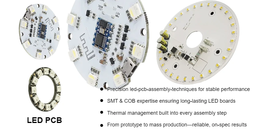
High-performance LED products are built on disciplined assembly, not guesswork. As Highleap PCB Factory—a PCB manufacturing + PCB assembly electronic factory—we combine DFM reviews, rigorous process control, and production-proven tooling to deliver repeatable optical output, tight color stability, and long service life. For speed and quality at scale, our automated SMT Assembly lines and one-stop Turnkey Assembly service take you from prototype to volume with traceability and reliability baked in.
Successful LED PCB assembly addresses thermal, optical, and reliability challenges at every step. From precise solder paste printing to optimized reflow and COB wire bonding, the methods below show how we engineer consistency into your build—so modules leave the line bright, uniform, and ready for demanding environments.
Solder Paste Printing Optimization
Precise solder paste application forms the foundation of reliable LED assembly, particularly for thermal pad connections.
Stencil Design for LED Applications: Thermal pad apertures require careful optimization balancing coverage with void prevention. We typically reduce aperture area to 80-90% of pad size, preventing excess paste that causes LED tilting. Window-pane or cross-hatch patterns divide large apertures into smaller sections, reducing void formation while maintaining thermal transfer. Rounded corners on apertures improve paste release, especially for fine-pitch designs.
Paste Selection and Management: Type 4 or Type 5 solder paste provides superior printing definition for miniature LED packages. No-clean flux formulations prevent residue affecting optical surfaces. Low-voiding paste formulations minimize thermal resistance under LED packages. Nitrogen storage and automated paste management maintain consistent viscosity. Regular viscosity testing ensures optimal printing throughout production runs.
Print Parameter Optimization: Squeegee pressure, speed, and separation parameters significantly impact paste deposition:
- Print speed: 25-50mm/s for consistent deposition
- Squeegee pressure: Minimum required for clean stencil
- Separation speed: 0.5-1.0mm/s prevents paste stretching
- Print gap: Contact printing for optimal transfer
Automated stencil cleaning every 10-15 prints maintains aperture clarity. Print verification using 3D solder paste inspection ensures consistent volume and placement.
Component Placement Strategies
Accurate LED placement ensures consistent optical performance and reliable solder joints.
High-Speed SMT Placement
Modern pick-and-place equipment achieves the precision required for LED arrays:
- Vision Systems: Upward-looking cameras verify component orientation before placement
- Placement Accuracy: ±25μm repeatability for consistent LED alignment
- Force Control: Programmable placement force prevents component or substrate damage
- Nozzle Selection: Specialized nozzles for various LED package types
Local fiducials near LED arrays compensate for substrate warpage. Automatic optical inspection after placement catches errors before reflow. Component verification systems prevent wrong part placement or polarity errors.
Manual and Semi-Automated Assembly
Some LED applications require manual or semi-automated assembly:
- Large COB LEDs exceeding automated equipment capabilities
- Prototype builds with frequent design changes
- Specialized components requiring careful handling
- Mixed technology boards with unique requirements
Microscope-assisted placement ensures accuracy for manual operations. Placement jigs and fixtures improve consistency and speed. Selective soldering systems handle through-hole LED components.
For compact, curved, or space-constrained light engines, we leverage Rigid-Flex PCB architectures and dense HDI PCB layouts to maintain alignment, reduce footprint, and keep routing short for current uniformity.
Reflow Soldering for LED PCBs
Temperature profile optimization balances complete solder melting with LED thermal limitations.
Profile Development: Each LED PCB design requires customized reflow profile development:
- Gradual preheating (1-2°C/second) prevents thermal shock
- Soak zone activates flux while equalizing temperature
- Reflow zone achieves complete solder melting without exceeding LED limits
- Controlled cooling prevents solder joint stress
Thermal profiling using multiple thermocouples validates temperature uniformity. Data logging systems record actual versus target temperatures. Profile adjustments compensate for thermal mass variations.
Nitrogen Atmosphere Benefits: Inert atmosphere reflow provides multiple advantages:
- Reduced oxidation improves solder wetting
- Lower peak temperatures possible with better wetting
- Decreased voiding under thermal pads
- Improved solder joint appearance and reliability
Oxygen levels below 100ppm provide optimal results. Cost-benefit analysis determines nitrogen usage for specific products.
Vapor Phase Soldering: Alternative to conventional reflow for temperature-sensitive LEDs:
- Maximum temperature limited by fluid boiling point
- Uniform heating regardless of component mass
- No oxidation in vapor atmosphere
- Ideal for high-mass or high-layer-count boards
For high-power arrays, pairing optimized profiles with the right stack-up—such as High-Thermal PCB substrates, Metal Core PCB (MCPCB) bases, or Ceramic PCB (AlN/Al₂O₃)—reduces junction temperature and improves lumen maintenance.
Chip-on-Board (COB) LED Assembly
COB technology enables high-density LED arrays with superior thermal performance.
Die Attachment Process
Precise die placement and bonding ensures reliability:
- Adhesive Selection: Silver-filled epoxy for thermal/electrical conduction
- Dispensing Control: Consistent bond line thickness for thermal transfer
- Die Placement: ±10μm accuracy for proper wire bond positioning
- Curing Process: Controlled temperature ramp prevents die stress
Automated die attach equipment handles high-volume production. X-ray inspection verifies bond line quality and coverage. Pull testing validates adhesion strength meets specifications.
Wire Bonding Techniques
Electrical connections require specialized wire bonding:
- Gold Wire Bonding: 25-50μm diameter for fine-pitch applications
- Aluminum Wire: Cost-effective for power connections
- Bond Parameters: Optimized force, time, and ultrasonic energy
- Loop Control: Consistent wire loops prevent shorting
Bond pull testing ensures wire bond strength exceeds specifications. Optical inspection verifies loop height and bond placement. Plasma cleaning improves bond pad adhesion.
Encapsulation and Phosphor Application
Protective encapsulation and phosphor coating complete COB assembly:
- Silicone encapsulants protect wire bonds from mechanical damage
- Phosphor mixing and dispensing for white light generation
- Dam-and-fill techniques contain encapsulant flow
- UV or thermal curing based on material selection
Color consistency requires precise phosphor concentration control. Optical testing validates color temperature and CRI.
Through-Hole LED Assembly
Through-hole LEDs remain essential when designs demand mechanical durability, precise optical alignment, or long-term serviceability. Unlike pure SMT solutions, through-hole mounting secures LEDs firmly to the PCB, making it the preferred option for automotive lights, industrial panels, and robust medical devices.
Wave soldering is the classic high-volume method, delivering full pin-to-hole fill with controlled flux, preheating, and nitrogen-assisted solder quality. For mixed-technology boards, selective soldering offers pinpoint precision—soldering individual joints without disturbing nearby SMT components. Both methods ensure strong joints, stable thermal paths, and consistent performance under demanding conditions.
For prototypes, specialty builds, or repairs, hand soldering remains valuable when done with strict temperature control and skilled operators. At Highleap PCB Factory, our Through-Hole Assembly integrates seamlessly with SMT and advanced processes, giving customers reliable LED PCBs that balance strength, flexibility, and production efficiency.
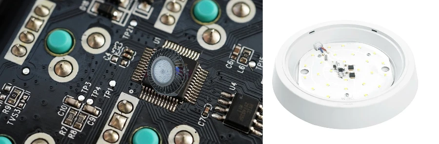
Quality Control in LED Assembly
Multiple inspection points ensure assembly quality and reliability.
Automated Optical Inspection (AOI)
Machine vision systems detect assembly defects:
- Component Presence/Absence: Verifies all LEDs placed
- Polarity Check: Ensures correct LED orientation
- Solder Joint Inspection: Identifies bridging, insufficient solder
- Alignment Verification: Confirms LED positioning accuracy
Multi-angle cameras inspect obscured areas. Color cameras verify LED types and values. Programming optimization reduces false calls while catching real defects.
In-Circuit Testing (ICT)
Electrical verification confirms circuit functionality:
- LED forward voltage measurement at specified current
- Leakage current testing for reverse bias conditions
- Driver circuit validation including current regulation
- Continuity testing of all circuit nodes
Flying probe testing for low-volume or prototype builds. Bed-of-nails fixtures for high-volume production. Boundary scan for complex digital circuits.
Functional Testing
Final validation under operating conditions:
- Light output measurement using integrating spheres
- Color temperature and CRI verification
- Thermal testing at rated power levels
- Dimming and control function validation
Burn-in testing accelerates infant mortality failures. Environmental stress screening identifies marginal assemblies. Statistical sampling plans ensure consistent quality.
Partner with LED Assembly Experts
As Highleap PCB Factory, we don’t just place LEDs—we industrialize light. Our DFM-first workflow, validated processes, and end-to-end documentation compress launch timelines and protect long-term reliability. Whether you’re building slim rigid-flex engines, dense HDI arrays, or high-power COB modules on MCPCB/ceramic bases, our team scales your product from pilot to mass production with confidence and control.
Ready to turn a design into a durable, production-grade light engine? Engage our process-proven team for rapid NPI and stable volume builds—backed by on-spec thermal performance, uniform optics, and automotive/medical-friendly traceability.
Q1: What's the minimum LED pitch you can reliably assemble?
A: We routinely assemble 0.5mm pitch LED arrays with specialized equipment and processes ensuring consistent quality.
Q2: How do you prevent LED damage during assembly?
A: Controlled temperature profiles, ESD protection, and moisture management prevent thermal and electrical damage during assembly.
Q3: Can you handle mixed LED types on the same board?
A: Yes, our assembly process accommodates multiple LED types, including different colors, packages, and power ratings on single boards.
Q4: What testing is included with LED assembly?
A: Standard assembly includes AOI and basic functional testing. Additional optical and thermal testing available per requirements.
Q5: Do you support LED binning and matching?
A: Yes, we provide LED binning services ensuring color and brightness consistency across arrays for uniform illumination.
Ready to Optimize Your LED Assembly?
Contact our assembly experts for consultation on your LED PCB project. We provide comprehensive solutions from prototype assembly through volume production with consistent quality and competitive pricing.