
Aluminum PCB & Metal Core PCB (MCPCB) Manufacturing | Copper Core Options | Thermal Path Engineering
Direct factory aluminum PCB and metal core PCB manufacturer for high-power LEDs, power conversion, and automotive systems. As an experienced aluminum circuit board and aluminum printed circuit manufacturer, HilPCB provides 1.0–8.0 W/m·K thermal dielectrics, 24-hour rapid prototyping from raw inventory, and volume pricing.
Capabilities
Aluminum PCB Thermal Path Optimization Through Material & Process Control
Balance dielectric thickness, thermal resistance and isolationWhen power density exceeds ~0.5–1.0 W/cm² or junction temperature limits are tight, the PCB must function as an active heat spreader. Standard FR-4 PCB provides only ~0.3–0.4 W/m·K of thermal conductivity. In contrast, an Aluminum PCB, aluminum pcb board, or specialized metal core PCB (MCPCB) integrates an aluminum or copper base with a ceramic-filled dielectric (typically 1–5 W/m·K) to lower thermal resistance and improve reliability under high-power load. As a direct metal core pcb manufacturer, HilPCB maintains standard raw laminate inventory for rapid turnaround.
Dielectric thickness—usually 75–150 μm—dominates thermal impedance (Rth) and determines breakdown voltage. Our vacuum lamination process holds thickness within ±10% and ensures dielectric integrity during thermal cycling. For hot-spot dissipation, stitch thermal-via arrays beneath power devices, or pair with heavy copper PCB layers to enhance lateral spreading. Explore detailed manufacturing methods in MCPCB assembly and thermal materials selection guides.
Critical Risk: Inadequate dielectric uniformity or metal-core warpage can cause local hotspots, breakdown, or solder fatigue under cyclic loading. Poor via insulation or delamination increases Rth by up to 30%, degrading LED lumen maintenance or MOSFET reliability.
Our Solution: We perform thermal shock testing (−40 °C↔+150 °C) and FEA-based heat modeling to validate conduction paths and mechanical stability. Surface flatness and dielectric bonding are monitored via SPC and CTE-matched stack-up design. For hybrid heat-spreading, see ceramic PCB alternatives that combine Al₂O₃/AlN with metal substrates to achieve conductivity up to 190 W/m·K.
For LED, EV converter, and industrial power systems, Aluminum PCB is often the first MCPCB option evaluated because it balances cost, thermal conductivity, and manufacturability. Learn more in our thermal management design series, which covers stack-up optimization, via density, and interface materials for efficient dissipation.
- System Rth targets <0.5 °C/W
- Dielectric uniformity ±10%
- Thermal vias Ø0.30–0.50 mm, 1.0–1.5 mm pitch
- Al core ~140–160 W/m·K; Cu core ~380–400 W/m·K
- White solder mask for LED reflectance >85%
🚀 Quick Quote Request
📋 Get Full Capabilities
Lamination Process Control & Reliability Validation
Void-free bonding and repeatable thermal resistanceVacuum lamination at staged pressure (typically 20–30 kg/cm²) and peak temperature 175–185 °C creates void-free interfaces and stable dielectric thickness. Pre-lam micro-etch targets Ra ~1–2 μm for adhesion without penalizing thermal contact. Panel temperature uniformity is held within ±3 °C.
Validation includes ASTM D5470 thermal measurements (acceptance ±15%), 100% Hi-Pot up to 4,000 V AC, and cycling −40↔+125 °C for 500–1,000 cycles with resistance change <10%. Learn more in thermal shock testing and board-level PCB testing.
- Void area typically <2%
- Temperature uniformity ±3 °C
- Peel strength ≥1.5 N/mm
- SPC on dielectric thickness and lamination pressure
- Lot retention and MES traveler records
Complete Technical Specifications for MCPCB
Thermal materials, isolation, and high-power routing
| Parameter | Standard Capability | Advanced Capability | Standard |
|---|---|---|---|
Layer Count | 1–2 layers | Up to 4 layers | IPC-2221 |
Base Materials | Aluminum 5052/6061 | Copper C110, Stainless options | Material spec |
Thermal Conductivity (system) | 1.0–3.0 W/m·K | Up to 8.0 W/m·K; copper core ~380–400 W/m·K | ASTM D5470 |
Dielectric Thickness | 75–150 μm | ≤50 μm high-performance | Manufacturer datasheet |
Board Thickness | 0.8–2.0 mm | 0.5–3.2 mm | IPC-A-600 |
Copper Weight | 1–3 oz (35–105 μm) | Up to 10 oz (350 μm) | IPC-4562 |
Min Trace/Space | 150/150 μm (6/6 mil) | 100/100 μm (4/4 mil) | IPC-2221 |
Min Hole Size | 0.30 mm (12 mil) | 0.20 mm (8 mil) | IPC-2222 |
Max Panel Size | 571.5 × 600 mm | 571.5 × 1200 mm | Manufacturing capability |
Breakdown Voltage | ≥3,000 V AC | ≥6,000 V AC | IEC 60243-1 |
Surface Finish | OSP, Lead-Free HASL | ENIG, Immersion Silver, ENEPIG | IPC-4552/4556 |
Quality Testing | E-test, Thermal Resistance | Thermal Cycling, Hi-Pot, TDR (as needed) | IPC-9252 |
Certifications | ISO 9001, UL, RoHS/REACH | IATF 16949, ISO 13485, AS9100 | Industry standards |
Lead Time | 5–10 days | 3–5 days expedited | Production schedule |
Ready to start your PCB project?
Whether you need simple prototypes or complex production runs, our advanced manufacturing capabilities ensure excellent quality and reliability. Get your quote within 30 minutes.
Design for Thermal Management (DFT) Implementation
Use copper spreading planes under heat sources and dense thermal-via fields: typical 50–100 vias/cm² with Ø0.30–0.50 mm and 1.0–1.5 mm pitch. For power paths and bus bars, consider heavy copper PCB. Keep sensitive RF/analog areas isolated with thermal slots; for RF PAs, evaluate ceramic PCB modules where conductivity and CTE match are critical.
Interface quality drives TIM performance: maintain local flatness within ±25 μm and Ra ≤3 μm across pad fields. For cost/lead-time trade-offs, see our PCB assembly quote guide.
Need Expert Design Review?
Our engineering team provides free DFM analysis and optimization recommendations
Multi-Stage Manufacturing with Quality Gates
Flow: substrate prep → dielectric application/lamination → pattern/etch → drill/plate (as required) → mask/finish → verification. Automated thickness mapping (9–25 points per panel) holds dielectric within ±10%. Ultrasonic C-scan/X-ray screens voids >0.5 mm with total void area typically <2%. Hi-Pot validates isolation per design voltage.
For assemblies mixing power and dense logic, hybridize with HDI PCB or backplane PCB where interconnect reach is required. Process windows and recipes are documented in our manufacturing flow.
Aluminum PCB, Copper Core & Dielectric Trade-offs
Aluminum PCB (5052/6061): ~140–160 W/m·K, CTE ~23 ppm/°C; best value for LEDs and moderate-power thermal designs.
Copper core: ~380–400 W/m·K, CTE ~17 ppm/°C; use for extreme flux or compact heat sources.
Dielectric: 1–2 W/m·K standard; 3–5 W/m·K advanced (processing adjustments required). Ultra-thin ≤50–75 μm reduces Rth but lowers isolation; we co-optimize thickness vs voltage. For module-to-system integration, see box build.
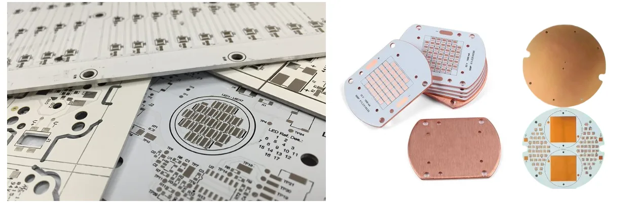
MCPCB Board Construction: Aluminum vs Copper Core and 1-Layer to 4-Layer Routing
The three practical forms of a metal core PCB differ by how much current-carrying and routing capability you need above the thermal path.
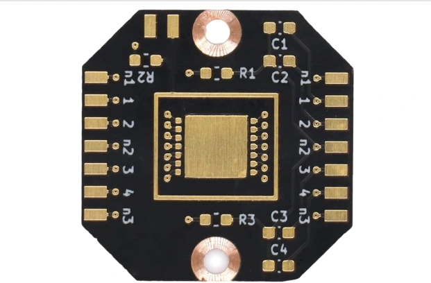
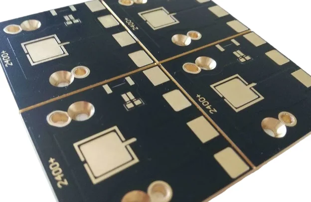
Single-layer aluminum MCPCB. One copper foil, dielectric, aluminum base. This is the classic aluminum MCPCB used for LED arrays and is the lowest-cost MCPCB that still removes heat through the base. Routing is planar, so crossovers are not possible — the layout must be single-sided by design, not by accident.
2-layer and 2–4 layer metal core PCB. A 2–4 layer metal core PCB (MCPCB) adds inner routing above the thermal core, which is what allows an aluminum-core assembly to carry control electronics on the same board as the power stage. Adding layers does not change the core's job; it changes how much gate-drive, sensing and protection circuitry can sit beside the heat source. The constraint shifts from thermal resistance to dielectric breakdown voltage across the added layers.
Copper core. Copper's ~380–400 W/m·K and lower CTE suit heat fluxes above 5–10 W/cm² and compact sources where aluminum's spreading limit binds. The cost is mass and machining; the benefit is that the base itself becomes the heat spreader. See heavy copper PCB when the requirement is copper thickness in the traces rather than the base.
A related family worth understanding is the thermal substrate or insulated metal substrate (IMS): same metal-base concept, described by the dielectric system rather than the core. When a datasheet says IMS, the engineering questions are identical to MCPCB — dielectric thickness, conductivity and bond integrity.
SPC, Batch Validation & Documentation
Incoming inspection verifies alloy, thickness and surface condition; dielectric lots get spot-checked via ASTM methods. SPC charts track dielectric thickness, void %, peel strength and thermal resistance with Cpk ≥1.33. First Article validation includes D5470, Hi-Pot and microsections; lot reports are retained for automotive/medical audits. See IPC Class 3 manufacturing for acceptance criteria.
LED, Power Conversion and Automotive
LED lighting: street/automotive lamps target junction-to-sink <1 °C/W using aluminum MCPCB and high-reflectance masks.
Power conversion: copper-core for IGBT/MOSFET modules with heat flux >5–10 W/cm².
Automotive: cycling −40↔+125 °C with traceability and PPAP readiness. For flexible jumpers near hot zones, pair with flex PCB.
Metal Core PCB LED and High-Power Designs: Sizing the Thermal Path
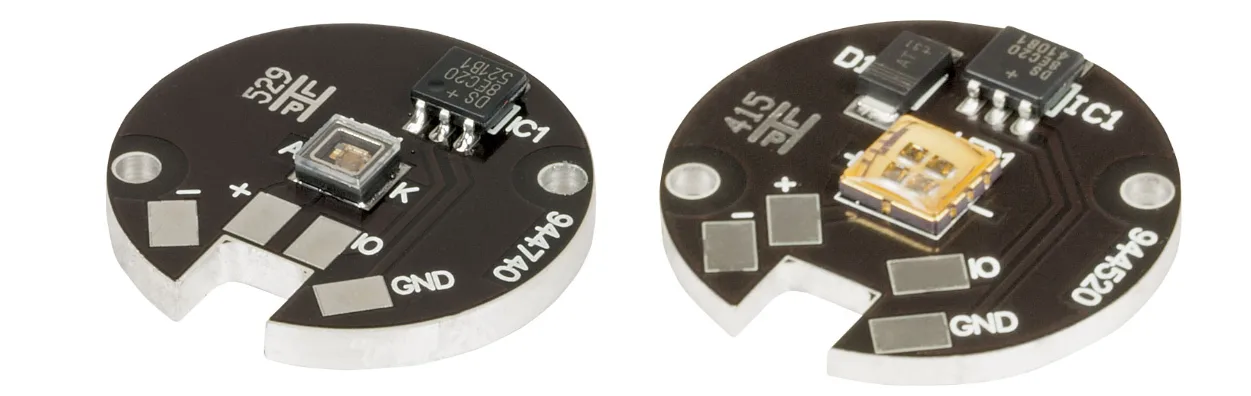
The most common request we receive is a metal core PCB for LED lighting, and the design question is almost always the same: how much copper area and how thin a dielectric are needed before junction temperature stops being the limiting factor.
Start from flux, not from board area. A metal-core LED design handling a few watts over a small emitter footprint may see local flux that overwhelms a 1 W/m·K dielectric regardless of how large the panel is, because spreading happens laterally in the copper. Across a panel of MCPCBs the same logic applies. Raising the dielectric to 3–5 W/m·K reduces the temperature drop across the bond line; increasing copper weight reduces the lateral drop. They solve different halves of the problem, which is why "upgrade the dielectric" is not always the answer.
For a high-power LED board, three parameters decide the outcome: dielectric thickness (75–150 µm standard, ≤50 µm high-performance), copper weight on the trace layer, and the density of thermal vias if the design uses them. Target junction-to-sink thermal resistance below 1 °C/W for street and automotive lamps, and verify it by measurement rather than by summing datasheet values.
Optics and solder mask interact with the thermal design. High-reflectance white mask improves light extraction but changes surface emissivity; where the board also radiates, that trade should be evaluated with the luminaire, not in isolation. For designs that must flex around a curved housing, compare flex PCB and rigid-flex PCB options before committing to a rigid metal core.
Choosing an MCPCB Manufacturer: What Separates a Metal Core PCB Supplier From a Broker
When you search for an MCPCB manufacturer, the term covers two very different operations: a plant that owns dielectric coating and vacuum lamination lines, and a trading company that passes your metal core PCB file to a third party. The difference shows up in the parameters that actually govern thermal performance, because those parameters are set by process, not by specification.
Four questions separate the two. First, who applies the dielectric? A real metal core PCB supplier controls coating thickness on its own line and can hold it within ±10%; a broker publishes a datasheet value it cannot influence. Second, what happens to a void? Void area is a lamination outcome — vacuum staging profile, peak temperature uniformity and pre-lam surface preparation decide it. Third, can the supplier alter the stackup for your flux? Moving from 100 µm to 75 µm dielectric changes thermal resistance measurably but also changes isolation margin, and only the plant can requalify that trade. Fourth, what evidence ships with the lot? ASTM D5470 thermal resistance, C-scan void maps and Hi-Pot records are produced where the boards are made.
For volume programs, confirm that incoming MCPCB materials are verified by lot (alloy grade, core thickness, dielectric conductivity) rather than by generic certificate. This is the point where FR-4-style purchasing habits cause trouble: a metal core board is only as good as the bond between core and dielectric, and that bond is not visible on a drawing.
Send the stackup you are considering — core alloy, dielectric thickness and target thermal resistance — through the MCPCB quote request and we will come back with the process window and the measured D5470 data for that build, so the thermal decision is made on numbers rather than on a datasheet claim.
Engineering Assurance & Certifications
Experience: volume MCPCB for LED and power electronics.
Expertise: vacuum lamination, copper-filled vias, flatness/Ra metrology; SPC on critical parameters.
Authoritativeness: IPC-6012 Class 2/3, IATF 16949, ISO 13485; audit-ready traveler and lot reports.
Trustworthiness: MES links supplier lots, serialization and thermal test data; documentation retained per customer requirement.
- Controls: lamination pressure/temperature windows, dielectric thickness, void %
- Traceability: lot codes, unit serialization, digital traveler
- Validation: D5470 thermal, Hi-Pot, thermal cycling and microsections
Frequently Asked Questions
MCPCB vs. standard FR-4: when should I migrate?
Aluminum or copper core—how do I choose?
How many thermal vias are needed under a power device?
What isolation voltages can you support?
Which finish is best for thermal pads and LEDs?
What is the MCPCB full form and what does it stand for?
Is an aluminum PCB the same as an MCPCB?
Experience Advanced PCB Manufacturing Excellence
From simple prototypes to complex production runs, our world-class factory delivers superior quality, fast turnaround and competitive pricing. Join thousands of satisfied customers who trust us with their PCB manufacturing needs.