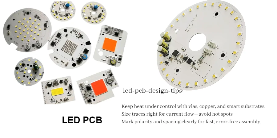
If you’re designing LED modules for automotive, street lighting, signage, or backlights, the fastest way to hit thermal, optical, and cost targets is to bake in led-pcb-manufacturing from day one. The guidelines below are distilled from thousands of builds—use them as a practical checklist to reduce respins, avoid hot spots and flicker, and shorten time-to-production.
Need the right base technology for your module? See: Metal-Core PCBs (MCPCB) · Ceramic PCBs · Flex PCBs · High-Thermal PCBs
Thermal Path: FR-4 vs. MCPCB (Don’t Treat Them the Same)
FR-4 LED PCBs
Use via-in-pad (filled & capped) or dense thermal-via fields directly under LED thermal pads to pull heat into backside copper/heatsinks. Typical starting points: 0.25–0.35 mm holes, 0.8–1.2 mm pitch tied to large copper pours. Keep conductor-to-edge clearance ≥0.5 mm (raise to ≥1.0 mm for high-voltage strips) to protect creepage and avoid burr shorts.
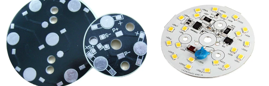
MCPCB / Aluminum or Copper Core
Do not rely on plated through-vias into the metal core. Optimize by specifying high-conductivity dielectric (≈1.0–5.0 W/m·K) with controlled thickness, enlarging copper spreading areas, and—where power is concentrated—using copper coins or embedded spreaders. For optical efficiency, specify white solder mask with ≥88% reflectance @ 550 nm (integrating-sphere measured, UV-stable formulation).
LED Spacing & Array Planning (Method First)
Start from power density (W/cm²) and target junction temperature rise (ΔTj), then choose spacing that your base material can support thermally and optically.
- Mid-power SMD on FR-4: begin with 2.5–3× package edge length as center-to-center spacing, then tune via protos or simulation.
- High-power LEDs on MCPCB: use 5–10 mm as a feasibility start, verify with thermal sampling under worst-case drive and ambient.
- Staggered arrays usually improve uniformity and reduce heat coupling vs. strict grids at equal part count.
- For linear/strip modules, alternating LED orientation can shrink loop area and cut EMI into driver sections.
Current Capacity & Voltage Drop (IPC-2152-Driven)
Size traces by allowable temperature rise and a voltage-drop budget (often limit total drop ≤3% from driver to the furthest LED). As a quick reference (1 oz copper, 25 °C ambient, natural convection—validate per your conditions):
| DC Current | Length ≤10 mm | Length 10–50 mm |
|---|---|---|
| 20–60 mA | 0.15–0.20 mm | 0.20–0.30 mm |
| 100–350 mA | 0.25–0.40 mm | 0.40–0.70 mm |
| ≥1 A (buses) | 0.80–1.50 mm | 1.50 mm+ or 2 oz copper |
Distribution matters: prefer star topologies from a low-impedance node over daisy chains to avoid visible brightness gradients. Add test points at rails/strings to accelerate ICT and functional checks.
For controlled-impedance driver/control sections, pre-size lines with the Impedance Calculator.
Pad, Mask & Marking (Built for Yield and Optics)
- Solder mask expansion: set +0.05–0.10 mm per side over copper pads to absorb registration errors while preventing bridging.
- COB/COB-like zones: add mask dams between bond pads to confine adhesive and keep die attach clean.
- White mask: specify ≥88% reflectance @ 550 nm and UV stability to resist yellowing over life.
- Teardrops: use at pad-to-trace transitions for mechanical robustness/manufacturability (not a primary thermal lever).
- Clear legends: polarity marks (symbol + text), current ratings/resistors near drivers, version/date codes in copper for permanent traceability.
Testability, AOI Fiducials & Panelization (Clean, Low-Stress)
- Access for test: expose voltage/current test pads per string; place global + local fiducials diagonally for AOI accuracy.
- Thermal sampling: put temperature probe pads near the worst-case LEDs for validation.
- Panelization:
- V-score for rectangles; tab-route + mouse-bites for irregular shapes.
- Mouse-bites: Ø0.6–0.8 mm, pitch 0.8–1.2 mm; keep parts ≥1.0–1.5 mm from board edge/bites.
- Add handling rails for SMT; remove after reflow/depanel.
Manufacturing-Ready Documentation (Go Fast, Avoid Rework)
Ship-ready LED PCBs start with a complete, unambiguous package. Use the checklist below to prevent holds, questions, and re-spins.
1) Source files & identifiers
- Manufacturing data: Gerber/ODB++, drill files, netlist (if available), and a brief README with build notes.
- Unique IDs: project name, revision, and date on every file; put rev/date in copper on the PCB for traceability.
- BOM (AVL-ready): MPN, refdes, quantity, DNP flags, and approved alternates; list LED bin/CCT/CRI by reference designator (e.g., D1–D10 = 3000K BIN 3).
- CPL/XY (pick-and-place): refdes, package, rotation, side, X/Y coordinates, units, and board origin.
- Pre-flight preview: verify layers/apertures before sending with the Gerber Viewer.
2) Fabrication notes (FR-4, MCPCB, Ceramic, Flex)
- Base selection: call out FR-4 / MCPCB / Ceramic / Flex with dielectric, total thickness, and copper weight (e.g., 1 oz / 2 oz).
- Stackup & targets: layer sequence, controlled-impedance requirements (if any), mask/legend colors.
- Edges & creepage: conductor-to-edge ≥0.5 mm (≥ 1.0 mm for high-voltage strips); define slots/chamfers/keep-outs.
- Solder mask & pads: mask expansion +0.05–0.10 mm per side; add mask dams in COB zones. Specify white mask ≥88% reflectance @ 550 nm (UV-stable).
- Panelization: panel size, V-score or tab-route + mouse-bites (Ø 0.6–0.8 mm, pitch 0.8–1.2 mm), rails/handling bars, fiducials (global + local).
- Markings: polarity “+/–”, voltage warnings, 1D/2D barcode (if required), and packing label fields (PN, lot, qty).
3) Thermal, current & optics intent
- Thermal targets: allowed ΔTj, hottest LEDs to sample, probe pad locations for temp logging.
- Current & voltage drop: state IPC-2152 sizing assumptions and a ≤3% end-to-end drop budget; note any 2 oz/3 oz copper buses.
- Optical criteria: uniformity/brightness goals, acceptable color shift, choice of white vs black mask for reflectance/glare.
4) Assembly instructions (LED-specific)
- Reflow/wave profiles: peak temp, soak/peak times; include MCPCB/ceramic profiles (high thermal mass).
- Stencil & paste: stencil thickness and apertures (use window-pane pattern on large thermal pads); paste alloy/flux type.
- Low-void target: define acceptance criteria for thermal pads (≤10–15% average voiding) and sampling method.
- LED handling: bin/CCT/CRI sampling plan, anti-mixing rules, lens/window handling notes.
- Special processes: conformal coating/potting (masking map), adhesives/encapsulants, torque/fastening, cure times.
5) Test & quality plan
- ICT/functional: test-point map, thresholds, PASS/FAIL windows; for constant-current drivers, specify current/voltage ranges.
- AOI/X-ray: criteria for large thermal pads/BGAs; AOI tolerances for rotation/text.
- Sampling & AQL: lot sampling percentage and AQL level; DOA handling and turn-around.
- Reliability (as needed): thermal cycle, damp-heat, salt-mist, and burn-in conditions/duration.
- Compliance pack: RoHS/REACH statements, UL file (if applicable), CoC/CoA, material traceability.
Quick DFM Checklist (Paste into Your PRD)
- Base tech chosen per power density (FR-4 + thermal vias / MCPCB / Ceramic / Flex)
- Target ΔTj & voltage-drop budget allocated; traces sized per IPC-2152
- White mask reflectance spec (≥88% @ 550 nm), legends & polarity marks confirmed
- Test pads/fiducials placed; rails & panel method (V-score or tab-route) selected
- Edge clearances & creepage distances reviewed (esp. HV strips)
- Bin/CCT mapping documented; void limits for thermal pads defined
- Files ready: Gerber/ODB++, BOM, CPL/XY, test plan; previewed in Gerber Viewer
- Assembly path locked (SMT or turnkey)
Partner with LED PCB Experts
Send your Gerber / BOM / CPL for a free 24-hour DFM. Your red-lined report will include:
- Thermal path recommendations (FR-4 vs MCPCB vs Ceramic) with actionable fixes—copper spreading, copper coins, dielectric choices.
- IPC-2152 trace review and voltage-drop budget tuning (star distribution vs daisy chain).
- Mask/stencil optimizations for low-void thermal pads (target ≤10–15%).
- Panelization & rails aligned to your depanel route (V-score vs tab-route) and line fixtures.
- Base technology guidance, including when to switch to Flex for tight envelopes or dynamic bend zones.
Need execution now? Our SMT Assembly and Turnkey Assembly teams take the DFM-clean package straight into build with predictable lead times, labeled per SKU, full QA records, easy payments, and tracked global delivery.