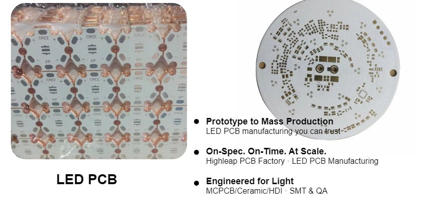
Standard PCB workflows can’t guarantee LED lifetime, color stability, or thermal margins. You need a purpose-built LED PCB manufacturing process that bakes in heat dissipation, optical consistency, and reliability from day one. At Highleap PCB Factory (PCB manufacturing + PCB assembly), we turn design intent into repeatable factory results—see our guide to led-pcb-manufacturing to understand the essentials we implement on every build.
From automotive headlights to architectural luminaires and high-pixel-density displays, our end-to-end flow—DFM, substrate engineering, LED-grade solder mask, nitrogen reflow, and optical/thermal validation—delivers consistent output, tight color, and fast cycle times from quick-turn prototypes to mass production.
Pre-Production Engineering and Design Verification
Manufacturing excellence begins before production with comprehensive design review and optimization.
Design for Manufacturing (DFM) Analysis: Our engineering team reviews your LED PCB design for manufacturability, identifying potential issues before production begins. We verify trace widths support required current levels, thermal vias adequately dissipate heat, and component placements optimize assembly efficiency. Stack-up recommendations ensure optimal thermal performance while maintaining cost targets. This proactive approach prevents costly redesigns and accelerates time-to-market.
Thermal Simulation and Optimization: Advanced finite element analysis predicts thermal performance before manufacturing. We model heat flow from LED junctions through PCB substrates to heat sinks, identifying hot spots and optimization opportunities. Thermal via placement, copper distribution, and substrate selection recommendations ensure LEDs operate within temperature specifications. Simulation results guide design modifications that improve reliability and lifetime.
Tooling and Fixture Preparation: Custom tooling ensures consistent quality across production runs. Precision stencils with optimized apertures control solder paste deposition on thermal pads. Assembly fixtures maintain board flatness during reflow, preventing warpage that affects LED alignment. Test fixtures provide reliable electrical contact for in-circuit and functional testing. Our Gerber viewer tool helps validate designs before tooling fabrication begins. Investing in proper tooling upfront ensures repeatable, high-quality production.
Material Preparation and Substrate Processing
LED PCB manufacturing begins with careful material selection and preparation, with substrate choice dramatically impacting thermal performance and reliability.
Aluminum Substrate Preparation
Metal core PCBs require specialized handling to ensure proper adhesion and thermal performance:
- Surface Treatment: Chemical cleaning removes oxidation and contamination from aluminum surfaces
- Micro-etching: Creates optimal surface roughness for dielectric adhesion
- Dielectric Application: Thermally conductive prepreg precisely laminated to aluminum base
- Copper Foil Lamination: Heavy copper (35-140μm) bonded for current carrying capacity
Temperature and pressure profiles during lamination critically affect thermal conductivity. Our process control maintains uniform dielectric thickness (±10μm) ensuring consistent thermal performance. Multiple lamination cycles may be required for thick copper or multiple layer designs.
FR-4 and Specialized Material Processing
Standard FR4 PCBs undergo conventional processing with modifications for LED requirements:
- Enhanced copper plating for improved current handling
- Controlled impedance for high-frequency LED drivers
- White solder mask application for maximum reflectivity
- Surface preparation for optimal solder mask adhesion
Ceramic substrates require diamond drilling and laser processing due to material hardness, offering superior thermal conductivity for high-power LED applications. For applications requiring exceptional thermal management, our high thermal conductivity PCBs provide optimal heat dissipation performance.
Circuit Formation and Patterning
Creating precise circuit patterns requires advanced imaging and etching processes optimized for LED current requirements.
Photolithography Process: Laser direct imaging (LDI) provides superior resolution compared to traditional photo-tools. Direct exposure eliminates film-related defects and enables quick design changes. Fine line/space capabilities down to 75μm support high-density LED arrays. Registration accuracy ±25μm ensures precise alignment across layers.
Etching and Plating: Controlled etching creates uniform trace profiles essential for consistent current distribution. For high-current LED applications, our heavy copper PCB technology supports copper thickness up to 10oz, ensuring adequate current carrying capacity without voltage drop. Differential etching compensates for undercut, maintaining designed trace widths. Surface roughness control optimizes solder mask adhesion.
Via Formation and Plating: Thermal vias beneath LED pads require special attention:
- Precision drilling with minimal burr formation
- Complete via filling to maximize thermal conductivity
- Copper plating thickness verification in via barrels
- Back-drilling for impedance control in high-speed sections
Solder Mask and Surface Finish Application
Surface treatments significantly impact LED PCB optical and assembly performance.
White Solder Mask for LED Applications
Reflectivity optimization maximizes light extraction efficiency:
- Material Selection: Titanium dioxide-based formulations achieve >88% reflectivity
- Application Control: Screen printing or spray coating for uniform thickness
- UV Curing: Optimized exposure ensures complete polymerization without yellowing
- Thickness Verification: 20-30μm thickness balances coverage with flexibility
Multiple coating passes may be required for optimal opacity. Surface texture affects both reflectivity and LED placement accuracy. Long-term stability testing validates resistance to UV degradation and thermal cycling.
Surface Finish Options
Proper surface finish ensures reliable LED assembly:
- ENIG (Electroless Nickel Immersion Gold): Excellent flatness for fine-pitch components
- OSP (Organic Solderability Preservative): Cost-effective for rapid production
- Immersion Silver: Good solderability with moderate shelf life
- HASL (Hot Air Solder Leveling): Economical but limited flatness
For COB applications, wire bondable finishes like ENEPIG provide aluminum wire compatibility. Selective plating allows different finishes on the same board optimizing cost and performance.
SMT Assembly and LED Mounting
Precise component placement ensures consistent LED performance across arrays, with specialized SMT assembly processes critical for LED reliability.
Solder Paste Printing: Stencil design critically affects thermal pad connections. Aperture reduction (80-90%) prevents excessive paste causing LED tilt. Window-pane patterns reduce voiding under thermal pads. Type 4 or 5 paste improves fine-pitch printing consistency. Automated inspection verifies paste volume and placement.
LED Placement and Alignment: High-speed pick-and-place machines achieve ±25μm accuracy. Vision systems verify LED polarity before placement. Consistent placement pressure prevents component damage. Nozzle selection optimized for various LED package types. Local fiducials near LED arrays improve placement accuracy.
Reflow Soldering Optimization: Temperature profiles balance complete solder melting with LED thermal limits:
- Gradual preheating prevents thermal shock
- Controlled ramp rates minimize component stress
- Peak temperature and time above liquidus carefully controlled
- Cooling rate affects solder joint reliability
Nitrogen atmosphere reduces oxidation improving solder joint quality. Conveyor speed and zone temperatures require optimization for each design.
Quality Control Throughout Manufacturing
Multiple inspection points ensure consistent quality throughout the manufacturing process.
In-Process Inspections
Real-time monitoring prevents defects from propagating:
- Post-etch inspection: Verifies trace width and spacing
- Post-drilling inspection: Confirms hole quality and position
- Solder mask inspection: Checks coverage and registration
- Pre-assembly inspection: Final verification before component mounting
Statistical process control tracks trends enabling proactive adjustments. Automated optical inspection reduces human error while improving throughput.
Post-Assembly Testing
Comprehensive testing validates LED PCB functionality:
- In-Circuit Testing: Verifies component values and connections
- Functional Testing: Confirms LED operation at rated conditions
- Optical Testing: Measures light output and color consistency
- Thermal Testing: Validates heat dissipation effectiveness
Boundary scan testing for complex digital circuits. Flying probe testing for prototype and small batch verification. Burn-in testing for reliability validation.
LED PCB Manufacturing Process — Detailed, Correct Flow
Below is the true, stage-by-stage flow from design intake to finished, assembled LED boards. Variant notes are included for FR-4/multilayer, MCPCB (aluminum base), and ceramic (DBC/AMB) builds.
1. Design Intake, CAM & Tooling
- DFM/DFT review, stack-up confirmation, thermal targets, pad/via rules, fiducials.
- Panelization (step-and-repeat, rails, tooling holes, coupons), impedance and copper balance checks.
- Generate drill/route files, LDI data, solder-mask/legend, E-test netlist; stencil & test-fixture specs released.
2. Incoming Quality Control (IQC)
- Verify laminate/metal base, copper weight, dielectric thickness & Tg; mask/ink/chemicals lot checks.
- LED BOM/ICs: MSL/date code, reel labeling, traceability.
3. Core Material Prep (by substrate)
- FR-4 / Multilayer: Inner-layer copper clean → LDI imaging → etch → inner-layer AOI → oxide/adhesion.
- MCPCB (Al base): Clean Al base → dielectric lamination (if not pre-laminated) → copper foil lamination.
- Ceramic (DBC/AMB): DBC tile IQC (AlN/Al₂O₃ with Cu) or perform bonding → surface prep.
4. Lamination / Bonding
- FR-4: Multilayer press (temperature/pressure/vacuum profiles) → cool → registration check.
- MCPCB: Press dielectric/Cu stack (if in-house) with tight dielectric thickness control for Rθ consistency.
- Ceramic: Post-bond stabilization bake as required.
5. Drilling & Via Formation
- Through/slot/controlled-depth drilling; FR-4 desmear (plasma/permanganate).
- HDI (if used): Laser microvias, sequential lamination.
- MCPCB: Typically no PTH through to aluminum core; use isolated vias only when designed for 2-layer MCPCB.
- Ceramic: Laser machining or thick-film vias when applicable.
6. Metallization & Copper Build-Up (FR-4 / HDI)
- Electroless Cu seed → electrolytic Cu plate (via barrels & outer layers).
- Pattern plate (if used) to target final copper thickness.
7. Outer-Layer Imaging, Etch & AOI
- LDI outer layers → develop/etch/strip → controlled trace geometry → outer-layer AOI (defects, width, spacing).
8. Solder Mask (LED-Grade White) & Legend
- Clean → apply high-reflectivity white mask (spray/screen) → image/cure to 20–30 µm.
- Reflectance/opacity check (avoid yellowing); keep keep-outs around optical windows.
- Apply legend/marking; final cure.
9. Surface Finish (per assembly & LED package)
- ENIG for flatness/fine pitch; ENEPIG for COB/wire-bond; OSP/Imm-Ag for cost/throughput.
- Thickness verification (Ni/Au/Pd as applicable), solderability test.
10. Profile, Route & Electrical Test (Bare PCB)
- Routing/V-score/drill final; deburr & clean.
- Flying-probe or bed-of-nails 100% E-test vs netlist; high-pot/insulation tests as required.
11. SMT Assembly (LED Mounting)
- Kitting & Bake: Bake moisture-sensitive LEDs/PCBs; verify reels & polarity.
- Stencil Printing: Optimized thermal-pad apertures (80–90% area; window-pane) → SPI checks.
- Pick-and-Place: ±25 µm placement accuracy; local fiducials for arrays; first-article signoff.
- Reflow: N₂ profile; controlled ramp/soak/TAL/peak to protect LEDs and limit voiding.
- Post-Reflow QC: AOI for polarity/bridges; X-ray (AXI) on high-power pads to control voids.
12. Mixed-Tech & Secondary Ops (as needed)
- Selective solder for THT optics, connectors, big heat-slug LEDs; mechanical fixtures to shield SMT.
- Heat-sink attach, adhesive staking, potting/encapsulation where specified.
13. Functional, Optical & Thermal Validation
- ICT/FCT on drivers and controls.
- Optical test: luminous flux, CCT/CRI, uniformity; flicker metrics (PstLM/SVM when required).
- Thermal test at rated power (IR/junction proxy, ΔT to heat sink); record lumen maintenance vs temp.
14. Environmental & Reliability (per spec)
- Burn-in/power cycling; thermal cycling; humidity (e.g., 85/85); vibration/ shock where required.
- Record SPC data and traceability (lot, board serial, reel IDs).
15. Conformal Coating, Cleaning & Final Assembly
- Selective coating avoiding lenses/emitters; cure & UV inspection.
- Ionic cleanliness if no-clean residues must be minimized for optical areas.
16. Final QA, Packing & Shipment
- Final visual & dimensional checks; sampling for destructive analysis if specified.
- ESD/Moisture-Barrier Bags with desiccant & HIC; labels with revision/trace codes.
- Documentation pack: CoC, test reports, DHR/traceability, handling guides.
Transform Your LED Innovation into Market Success
Speed wins only when quality scales. Highleap PCB Factory integrates design review, fabrication, assembly, and verification into one disciplined flow, de-risking launches and delivering on-spec boards at any volume.
Choose our turnkey assembly services to streamline sourcing, build, test, and packaging with full traceability and automotive/medical-ready QA. Send your files for same-day DFM and we’ll convert your concept into production-ready light engines—on schedule, at scale, and built to last.