Multilayer PCB Cost Considerations
When evaluating multilayer PCBs for buying circuit boards, cost is often a deciding factor. Unlike single- or double-layer boards, multilayer designs involve more materials, advanced equipment, and complex process control, all of which directly affect pricing. Understanding these cost drivers helps customers make better decisions when planning production.
Key Factors Affecting Cost
- Layer Count — More layers mean more lamination cycles, drilling, and alignment steps. A 12-layer PCB can cost several times more than a 4-layer version.
- Board Size and Thickness — Larger panels or special thickness requirements increase material usage and machining time.
- Material Selection — Standard FR4 is cost-effective, while high-frequency laminates (Rogers, Taconic) and polyimide substrates significantly raise costs.
- Technology Level — Features like HDI microvias, via-in-pad, or controlled impedance add processing steps and raise unit prices.
- Surface Finish — ENIG, immersion silver, or OSP offer different performance levels but also different cost structures.
- Production Volume — Prototypes and small batches cost more per unit due to setup costs, while mass production reduces the average unit price.
Cost Optimization Strategies
- Standardize stackups where possible to reduce customization.
- Choose cost-effective materials unless high-frequency or thermal requirements demand otherwise.
- Optimize design for manufacturing (DFM) to avoid unnecessary via structures or exotic features.
- Plan production volumes strategically—larger batches deliver significant savings.
By balancing performance requirements with cost-effective design and manufacturing choices, customers can achieve the right trade-off between budget and reliability in multilayer PCB projects.
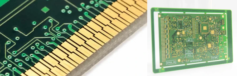
Multilayer PCB Capabilities
From basic 4-layer to advanced 60+ layer designs
Precise controlled impedance for high-speed signals
Precision microvias for high-density interconnect
Support for microwave and mmWave applications
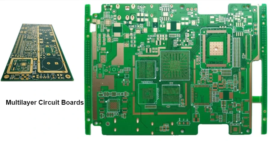
What is a Multilayer Circuit Board?
A multilayer circuit board integrates multiple conductive and insulating layers into a single rigid structure, typically ranging from 4 to 20+ layers depending on complexity. This architecture enables compact layouts, stable signal integrity, and efficient power distribution. The core characteristics of multilayer PCBs include:
- Laminated stackup combining signal layers, power planes, and ground planes for high-density interconnections
- Enhanced electromagnetic compatibility (EMC) through dedicated shielding layers
- Optimized impedance control critical for high-speed and RF circuits
- Increased wiring density for miniaturized devices and advanced system integration
Multilayer PCB construction relies on carefully chosen materials tailored to application requirements. Common choices include FR4 for cost-effective designs, Rogers/Taconic for high-frequency telecommunications, and polyimide for aerospace or automotive systems requiring high thermal stability. By combining advanced stackup design with the right substrate, manufacturers achieve boards that deliver performance, durability, and reliability for demanding industries.
Multilayer Circuit Board Manufacturing Process
Producing a multilayer PCB involves strict process control and multiple precision steps integrated with circuit board manufacturing workflows. Below is the conventional workflow used in professional PCB factories:
- Material Cutting (Panel Cutting) → Cutting raw laminates into required panel sizes
- Post-Cutting Baking → Baking the panels to remove moisture and stabilize dimensions
- LDI Registration Holes → Laser Direct Imaging (LDI) to define precise registration points
- Inner Layer Dry Film Application → Applying dry film photoresist to inner copper layers
- Inner Layer Etching → Etching unwanted copper to form circuit patterns
- Inner Layer AOI → Automated Optical Inspection for defects on inner layers
- Brown Oxidation → Oxidizing inner copper surfaces to improve adhesion
- Lamination → Pressing together inner layers, prepreg, and copper foil under heat and pressure
- Aluminum Entry Drilling → Using aluminum entry sheets for precision drilling of through-holes and slots
- Deburring → Removing burrs and resin residues from drilled holes
- Electroless Copper Deposition → Depositing a thin copper layer onto hole walls (PTH formation)
- Panel Plating (Electroplating) → Electrolytic copper plating to build hole wall thickness
- Negative Dry Film Application → Coating panels with dry film for outer layer patterning
- Dry Film Inspection → Checking registration and coverage accuracy
- Pattern Plating → Electroplating copper onto circuit traces and pads as defined by the dry film
- Outer Layer Etching → Removing excess copper, leaving final circuit patterns
- Outer Layer AOI → Inspecting for defects such as shorts, opens, or misalignment
- Surface Grinding → Mechanical brushing or polishing to prepare surfaces
- Solder Mask Application (Including Via Plugging) → Applying photoimageable solder mask with optional via plugging
- Solder Mask Inspection → Checking for proper coverage, alignment, and openings
- Silkscreen Printing → Adding reference designators, markings, and legends
- Surface Finishing → Applying HASL, ENIG, or other finishes to protect pads and ensure solderability
- Impedance Testing (if required) → Verifying impedance-controlled traces for high-speed designs
- Electrical Testing → Continuity and isolation tests to verify circuit integrity
- Profile Milling (Secondary Drilling, V-CUT) → CNC routing, milling, or V-scoring boards into final dimensions
- Functional Testing → Validating operational performance under load conditions
- Final Inspection → Checking cosmetic and dimensional quality
- Packaging → Vacuum packing and moisture protection for shipment
- Finished Goods Warehouse → Storage prior to logistics and delivery
Multilayer PCB Assembly and Testing Across the Entire Process
At Highleap PCB Factory, we ensure reliability through complete testing and quality control from manufacturing to final assembly. Every multilayer PCB goes through strict inspection at each stage:
- Manufacturing Testing: Electrical continuity, isolation, and impedance verification during fabrication, supported by AOI, X-ray, and microsection analysis for multilayer integrity.
- Final Manufacturing Validation: Thermal cycling, humidity, vibration, and dimensional inspections ensure the bare board meets industry reliability standards before circuit board assembly.
- Assembly Capabilities: High-speed SMT, through-hole, reflow, and wave soldering processes for complex multilayer PCBs, with full component sourcing and supply chain support.
- Post-Assembly Testing: Comprehensive ICT, functional testing, boundary scan, AOI, and X-ray inspections confirm that every assembled board performs exactly as specified.
This end-to-end process guarantees that customers receive multilayer PCBs that are not only manufactured to precise standards but also fully assembled, tested, and ready for integration into final products. Our comprehensive circuit board testing services ensure every aspect of performance is validated.
Choosing a Reliable Multilayer PCB Manufacturer in China
Selecting the right manufacturer is critical for ensuring multilayer PCB performance, cost efficiency, and long-term reliability. A trusted partner should demonstrate technical capability, strict quality systems, and full lifecycle support when buying circuit boards.
- Manufacturing Precision: Certified ISO/IPC processes, advanced equipment, and stable process control to guarantee consistent results.
- Highleap PCB Factory Expertise: Over 15 years of experience, multilayer capability up to 20+ layers, HDI and via-in-pad technology, plus in-house testing such as AOI, X-ray, impedance, and burn-in.
- End-to-End Services: From custom circuit board design to circuit board assembly and large-scale manufacturing, Highleap provides a complete solution under one roof, reducing lead times and simplifying project management.
With global shipping support and responsive engineering service, Highleap PCB Factory delivers multilayer circuit boards that meet demanding industry requirements while ensuring smooth project execution from prototype to mass production.