A single missed defect in production creates exponential costs. Finding a solder bridge during assembly costs $2. Finding it after conformal coating costs $20. Finding it in the field costs $200+ in warranty, returns, and reputation damage. Proper inspection catches problems at the right stage before costs multiply.
But not all inspection methods suit all situations. Understanding which inspections prevent problems versus which waste money helps optimize your quality strategy without over-spending on unnecessary procedures.
When Manual Inspection Still Matters (and When It Doesn't)
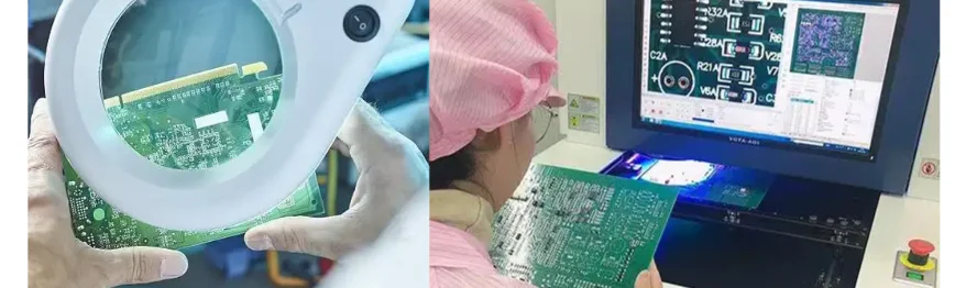
Automated inspection systems catch 95% of defects reliably. The remaining 5% often gets found by experienced human inspectors who notice subtle issues machines miss. But manual inspection has serious limitations that make it unsuitable as sole inspection method for volume production.
What Manual Inspection Catches
Trained inspectors under magnification identify:
- Mechanical damage to boards or components that affects fit in enclosure
- Subtle component misalignment that might not violate automated thresholds but indicates process drift
- Contamination issues (flux residue, handling damage, foreign material)
- Cosmetic defects affecting customer perception
- Context-specific problems requiring judgment automated systems lack
Inspection speed: 2-5 minutes per board with experienced inspector. Quality depends heavily on inspector training, fatigue, and consistency.
The Manual Inspection Reality
Problems emerge during long production runs:
- Inspector fatigue causes miss rates to increase after 4-6 hours
- Consistency varies between inspectors and shifts
- Cannot see hidden joints under components
- Subjective criteria lead to interpretation differences
- Documentation limited to inspector notes versus automated image capture
Manual inspection works as primary method only for small batches under 50 boards. Volume production requires automated inspection with manual inspection as supplement for catches what automation misses.
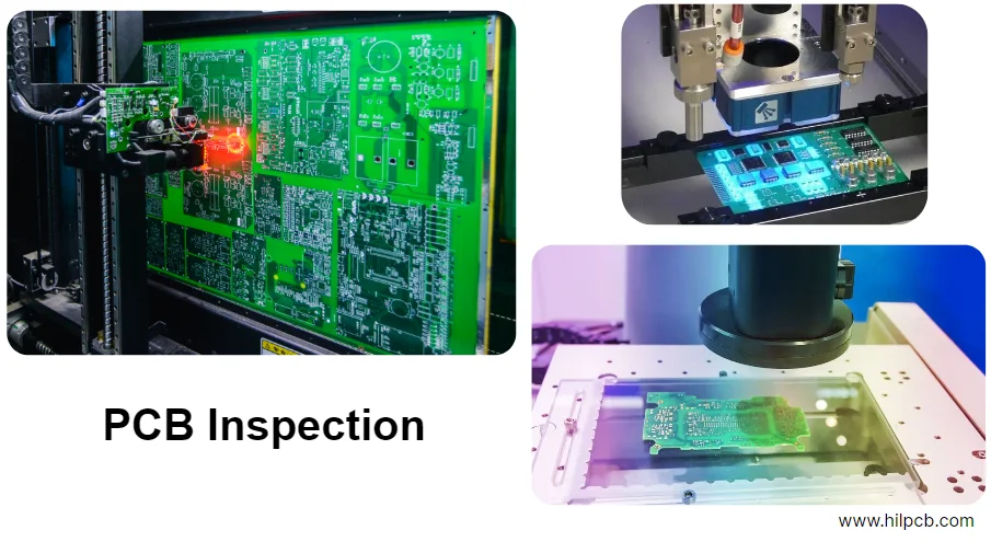
Automated Optical Inspection: What It Actually Catches
AOI systems use high-resolution cameras to capture board images and compare against golden board references or design databases. But "100% AOI inspection" doesn't guarantee perfect boards - understanding what AOI catches versus misses helps set realistic expectations.
Solder Joint Defects AOI Detects Reliably
- Insufficient solder: Joint appears starved, wicks up component lead instead of forming proper fillet
- Excess solder: Solder balls or connections appear oversized, potentially bridging adjacent pads
- Solder bridges: Solder shorts between adjacent pins or pads
- Missing solder: Pad appears bare without solder coverage
- Component issues: Parts missing, wrong polarity, rotated orientation, wrong components installed
Detection rates exceed 95% for these defect types when AOI system is properly programmed and maintained.
What AOI Cannot See
- Solder joints under BGA packages, QFNs, or inside connectors - requires X-ray
- Cold solder joints that appear visually acceptable but lack proper intermetallic bond
- Internal defects in multilayer boards - delamination, internal shorts, via failures
- Electrical functionality - component values, proper operation, firmware execution
AOI complements but doesn't replace electrical testing or X-ray inspection for complete quality assurance. Our PCB assembly process uses AOI after reflow as first-pass defect detection, followed by additional testing methods based on board complexity.
The False Positive Problem
Overly sensitive AOI settings flag acceptable boards as defective, slowing production:
- Slight component rotation within tolerance triggers false rejects
- Normal solder fillet variation gets flagged as insufficient/excess
- Reflections or lighting variations create false bridge detections
- Board warpage causes focus issues leading to false calls
Proper AOI programming balances sensitivity to catch real defects versus specificity to avoid false positives. Initial programming requires 2-4 hours per new board design with sensitivity tuning based on actual production results.
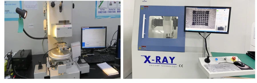
X-Ray Inspection for Hidden Solder Joints
BGA packages, QFN thermal pads, and connector pins create solder joints invisible to optical inspection. X-ray penetrates component bodies to image these critical connections - the only non-destructive method to verify joint quality.
Critical Defects X-Ray Inspection Reveals
Void Analysis: Solder voids reduce thermal and mechanical reliability. IPC standards specify maximum acceptable void percentages:
- Individual solder balls: <25% void area acceptable
- Thermal pads: <15% void area for power devices
- High reliability applications: <10% void area
Excessive voids cause:
- Reduced heat extraction from thermal pads leading to overheating
- Mechanical weakness increasing failure risk under thermal cycling
- Electrical resistance increase affecting power delivery
BGA Bridging Detection: Solder bridges between adjacent balls create short circuits optical inspection cannot see. X-ray reveals:
- Bridge presence and severity
- Affected ball locations
- Root cause analysis (excessive solder, pad design, reflow profile issues)
Insufficient Solder or Missing Balls: Ball collapse, non-wetting, or paste shortage creates weak or missing connections. X-ray shows:
- Individual ball quality across entire package
- Ball height uniformity indicating proper reflow
- Package centering on pad pattern
When X-Ray Inspection Becomes Mandatory
IPC Class 2 and Class 3 standards require X-ray inspection for:
- All BGA and similar area array packages
- QFN packages with central thermal pads
- Bottom-terminated components without visible leads
- Critical solder joints in high-reliability applications
Our PCB manufacturing process includes X-ray inspection of all BGA and hidden joint components with detailed reports showing void percentages and joint quality for each inspected component.
First Article Inspection: Validating Before Volume Production
First article inspection (FAI) thoroughly validates the first production units before committing to volume manufacturing. Catches design or process issues while corrections remain simple and inexpensive.
What First Article Inspection Includes
Dimensional Verification:
- Board outline dimensions and tolerances
- Hole locations and diameters
- Component placement accuracy
- Connector alignment and mechanical fit
- Overall assembly conformance to mechanical drawings
Electrical Verification:
- Net connectivity testing verifying all connections
- Impedance measurement for controlled impedance traces
- Power distribution voltage drop analysis
- High-speed signal quality assessment
- Functional testing under specified operating conditions
Materials Verification:
- Confirm specified materials used (FR4 grade, copper weight, surface finish)
- Verify component manufacturers and part numbers
- Check solder mask and silkscreen quality and legibility
- Validate conformal coating or other protective finishes
Process Validation:
- Reflow profile verification and documentation
- Soldering quality assessment per IPC-A-610 standards
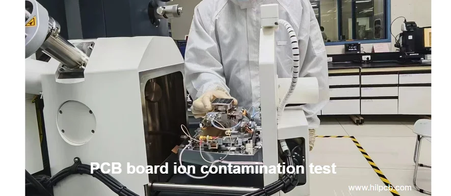
- Cleanliness testing for contamination
- Workmanship evaluation
Documentation package includes:
- Dimensional inspection reports with measurements
- Electrical test results and waveforms
- Material certificates and traceability
- Process parameters and settings
- Photographic evidence of critical features
How First Article Inspection Prevents Production Problems
Recent example: Customer's first article revealed connector alignment issue causing 0.5mm offset. Would have affected all 5,000 production boards. Design correction implemented before volume production prevented $15,000+ in rework costs.
Another case: Impedance testing during first article showed 58 ohms versus 50-ohm target. Stackup adjustment resolved issue before production commitment. Without first article verification, entire production batch would have required rework or scrap.
Microsection Analysis for Via and PTH Quality
Microsection analysis cuts boards and polishes cross-sections for microscopic examination of internal structures. Only method to verify plating quality, via filling, and layer-to-layer connections in multilayer boards.
What Microsection Analysis Reveals
Via Plating Quality:
- Plating thickness uniformity from top to bottom
- Coverage in high aspect ratio vias
- Plating voids or thin spots indicating process issues
- Copper thickness variation affecting reliability
Layer Registration:
- Alignment between layers affecting pad-to-via connections
- Annular ring uniformity confirming manufacturing capability
- Internal layer pad capture ensuring reliable connections
Material Quality:
- Delamination between layers indicating lamination problems
- Resin distribution and coverage
- Copper-to-laminate adhesion quality
- Internal defects not visible from surface
Typical Microsection Locations:
- High aspect ratio vias (>8:1)
- Critical signal vias in high-speed designs
- Thermal vias under power components
- Blind and buried vias in HDI boards
- Representative areas for each via type
Analysis typically requires 2-3 days including sample preparation, sectioning, polishing, imaging, and reporting. Performed on first article inspection and periodically during production for ongoing validation.
Complete PCB Inspection and Quality Assurance Capabilities
HILPCB provides comprehensive PCB inspection and testing coverage across the entire production process—from raw material verification to final product validation. Our inspection system supports both bare PCB fabrication and PCB assembly (PCBA), ensuring consistent quality, full traceability, and compliance with IPC and ISO standards.
Full Range of PCB Inspection and Testing Capabilities:
- Incoming Material Inspection (IQC): Verification of copper foil, prepreg, laminate, solder mask, surface finish, and component quality.
- Inner Layer Inspection: Optical alignment and AOI scanning for inner layers before lamination.
- Drilling and Plating Inspection: Hole size accuracy, via wall quality, plating thickness uniformity, and aspect ratio validation.
- Lamination and Registration Inspection: Layer-to-layer registration accuracy and resin flow control.
- Etching and Line Width Measurement: Verification of trace width, spacing, and conductor integrity per design tolerance.
- Surface Finish Inspection: ENIG, HASL, OSP, immersion silver/tin quality check for coverage, thickness, and oxidation.
- Solder Mask and Silkscreen Inspection: Alignment accuracy, thickness, and adhesion.
- Electrical Testing (E-test): 100% open/short test, insulation resistance, and high-voltage breakdown testing.
- Impedance Control Verification: Measurement of controlled impedance traces for high-speed and RF PCBs.
- Solderability and Peel Strength Testing: Ensures pad adhesion and plating reliability.
- Thermal Stress and T260/T288 Testing: Validates thermal endurance of multilayer structures.
- Cross-Section (Microsection) Analysis: Evaluation of copper plating, via quality, and internal structure consistency.
- Cleanliness and Ionic Contamination Testing: Confirms surface purity for high-reliability applications.
- AOI Inspection (Pre- and Post-Reflow): Automated optical checks for component placement, polarity, and solder joint integrity.
- 3D Solder Paste Inspection (SPI): Measures solder volume and uniformity before reflow.
- X-Ray Inspection: Detects internal solder joints under BGA, QFN, and multilayer voids or bridges.
- Functional and Boundary Scan Testing: Ensures logic, communication, and power systems operate as designed.
- First Article and Final Inspection: Full dimensional, electrical, and visual validation before shipment.
- Reliability and Environmental Testing: Includes thermal shock, vibration, humidity, and life-cycle testing for critical industries.
Each inspection record is electronically documented with corresponding test data, images, and material traceability for complete lifecycle tracking. This ensures every printed circuit board—whether rigid, flexible, HDI, or hybrid—meets the most demanding customer and industry standards.
As a PCB and PCBA manufacturer, HILPCB delivers integrated fabrication, assembly, and inspection solutions that combine precision, speed, and reliability—helping clients minimize risk, reduce total cost, and maintain product integrity from prototype through mass production.