
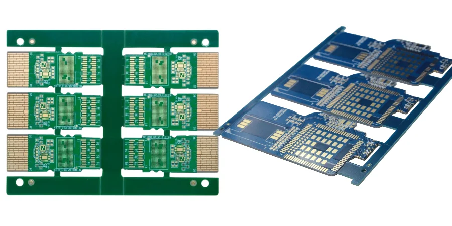
With the exponential growth in global data traffic driven by AI, cloud computing, and high-definition streaming, data centers are undergoing a rapid evolution from 100G/200G to 400G, 800G, and even higher speeds. In this bandwidth revolution, the QSFP-DD (Quad Small Form Factor Pluggable Double Density) optical module has become the core component of next-generation high-speed networks due to its high density, high bandwidth, and backward compatibility. However, cramming extreme performance into such a compact footprint presents unprecedented engineering challenges.
Ensuring the reliability and performance of these modules is no simple task. QSFP-DD module PCB testing is the critical barrier determining whether a product can be successfully commercialized. It is no longer just about basic continuity and short-circuit testing; it requires a systematic verification encompassing high-speed signal integrity, precise power delivery, extreme thermal management, and complex protocol compliance. This article will delve into the core challenges of QSFP-DD module PCB testing and explore how to ensure exceptional QSFP-DD module PCB quality through rigorous verification strategies.
High-Speed Signal Integrity (SI) Testing: The PAM4 challenge
The transition to 400G/800G is largely attributed to the adoption of PAM4 (Pulse Amplitude Modulation 4-level) technology. Unlike traditional NRZ (Non-Return-to-Zero) encoding, PAM4 transmits two bits of data per symbol cycle, effectively doubling the data rate without increasing the baud rate. However, the trade-off is a significantly smaller signal eye diagram—only 1/3 the height of NRZ—making the signal extremely sensitive to noise, jitter, and attenuation.
In QSFP-DD module PCB layout and testing, verifying PAM4 signal integrity is the top priority:
- Insertion Loss and Return Loss Testing: Utilizing a Vector Network Analyzer (VNA) to measure the S-parameters of the high-speed channels on the PCB. It verifies if the insertion loss of a
low-loss QSFP-DD module PCBfalls within the design budget and if the return loss meets standard requirements to prevent signal reflection. - TDR (Time Domain Reflectometry) Impedance Testing: Precise impedance matching is the foundation of high-speed signal transmission. TDR is used to detect impedance variations along the transmission line, specifically identifying impedance discontinuities at vias, connector pads, and BGA fan-out areas, which are major culprits for signal reflection.
- Eye Diagram and BER (Bit Error Rate) Testing: Feeding PAM4 signals into the module and observing the eye diagram at the receiving end using a high-speed oscilloscope. Key metrics evaluated include eye height, eye width, and TDECQ (Transmitter and Dispersion Eye Closure Quaternary). Additionally, a BERT (Bit Error Rate Tester) is used to verify if the link's error rate meets the stringent requirements (usually with Forward Error Correction, FEC) under worst-case conditions.
Power Delivery Network (PDN) Testing: Pursuing absolute purity
The internal power environment of a QSFP-DD module is extremely harsh. It houses highly power-hungry DSP (Digital Signal Processor) chips alongside highly noise-sensitive analog components like lasers (e.g., EML or Silicon Photonics) and TIAs (Transimpedance Amplifiers). This demands a highly stable and pure Power Delivery Network (PDN).
- Voltage Ripple and Noise Testing: When the DSP operates at full load and switches states dynamically, it generates significant high-frequency noise. If this noise couples into the power supply of the laser or TIA, it will directly degrade optical signal quality. Testing must employ high-bandwidth oscilloscopes and dedicated power rail probes to measure voltage ripple across different frequency bands, ensuring they remain within the strict tolerances defined by the chip manufacturer.
- Transient Response Testing: Simulating sudden load variations in the module to test the dynamic response capability of the power supply circuit. This verifies whether the power system can quickly recover to the nominal voltage without causing system resets or data errors when current demands spike.
- DC Voltage Drop (IR Drop) Testing: Given the module's small size, power traces are often narrow. High currents passing through these traces can cause significant voltage drops. Testing verifies that the actual voltage reaching the chip pins meets the minimum operating voltage requirements.
Thermal Performance Testing: A matter of life and death
Thermal management is the most critical physical bottleneck for QSFP-DD modules. The power consumption of 400G modules often reaches 12W-15W, while 800G modules can exceed 20W. Dissipating such massive heat within an incredibly confined space is an immense challenge.
QSFP-DD module PCB reliability is heavily dependent on thermal performance:
- Thermal Imaging and Thermocouple Testing: Operating the module under full load and using an infrared thermal imager to capture the temperature distribution across the PCB surface, identifying "hot spots." Furthermore, micro-thermocouples are attached to key components (like DSPs and lasers) to accurately measure their operating temperatures.
- Thermal Resistance Testing: Evaluating the efficiency of heat transfer from the chip to the module casing. This verifies the effectiveness of thermal vias in the PCB design and the thermal conductivity of Thermal Interface Materials (TIM).
- High-Temperature Operating Life (HTOL) Testing: Continuously operating the module in a high-temperature environment (e.g., 70°C or 85°C) to accelerate aging. This verifies long-term stability and exposes potential thermal-induced failure mechanisms, such as component parameter drift or solder joint fatigue.
Functionality and Protocol Compliance Testing: The soft power
A QSFP-DD module is not just a physical hardware device; it runs complex firmware to manage internal states and communicate with the host system (e.g., switches, routers).
- CMIS (Common Management Interface Specification) Compliance Testing: QSFP-DD modules must strictly adhere to the CMIS protocol for I2C (or MDIO) communication with the host, responding to commands and reporting statuses.
- Digital Diagnostic Monitoring (DDM): Real-time monitoring of key internal parameters, such as temperature, Vcc voltage, laser bias current, and received optical power (Rx Power).
- Initialization and Control: Configuring DSPs and other chips upon power-up, and controlling functions like laser switching and loopback testing based on host commands.
A significant portion of QSFP-DD module PCB testing involves functional and protocol compliance. Test platforms simulate host systems to perform comprehensive read/write operations on the module via the I2C/MDIO interface, verifying whether its memory map complies with CMIS specifications, the accuracy of DDM data, and the correctness and timeliness of responses to various control commands. This ensures the module's "soft power" and serves as the final gateway for delivering a high-quality product.
From Prototype to Mass Production: HILPCB's Value in QSFP-DD Module PCB Manufacturing and Assembly
Faced with the extreme complexity of QSFP-DD module PCBs, selecting a partner with both deep technical expertise and strong manufacturing capabilities is crucial. Leveraging long-standing experience in optical communications, HILPCB provides customers with a one-stop solution from prototype to mass production.
- Advanced Manufacturing Capabilities: We deeply understand the importance of a
low-loss QSFP-DD module PCBand offer industry-leading low-loss materials and precision manufacturing processes. Whether dealing with complex stack-ups, strict impedance tolerances, fine-line routing, or high-precision backdrilling, we ensure the final PCB perfectly meets design requirements, guaranteeing exceptionalQSFP-DD module PCB quality. - Flexible Prototyping Services: During product R&D, rapid iteration is key to success. We support
QSFP-DD module PCB low volumeproduction needs, offering rapid prototyping and Small Batch Assembly services to help customers accelerate their development process and shorten time-to-market. - Precision Assembly Processes: Optical module SMT assembly demands extremely high precision. Our SMT assembly lines are equipped with advanced mounters and inspection equipment capable of handling ultra-micro components like 01005s and high-pin-density BGAs. We can also collaborate with customers for the precision assembly of specialized components like optical engines.
By partnering with HILPCB, you can focus your energy on core chip and optical design, while we utilize our professional PCB manufacturing and assembly services to ensure your QSFP-DD module PCB layout is flawlessly realized and maintains long-term reliability in demanding application environments.
📋 QSFP-DD Module PCB Testing: Key Engineering Sign-off
Ensuring determinism and consistency of photoelectric conversion in 400G/800G network environments
Core Focus: For single-channel 56G/112G signals, test S-parameters and TDR impedance via VNA. The primary goal is controlling TDECQ (Transmitter and Dispersion Eye Closure Quaternary) and eliminating standing wave interference caused by via stubs.
Core Focus: Evaluating power supply ripple for the DSP and laser driver. Due to the high density of QSFP-DD ports, controlling DC IR Drop and dynamic impedance is mandatory to prevent ripple coupling from causing excessive jitter.
Core Focus: Under high power consumption (Class 1-8) conditions, measure actual chip junction temperatures. Utilize thermal via arrays and efficient casing conduction to ensure lasers do not suffer wavelength drift or accelerated aging due to localized heat accumulation.
Core Focus: Verifying the mechanical endurance of gold fingers and precision optical interfaces. Ensuring circuit design fully complies with CMIS (Common Management Interface Specification) to guarantee interoperability across various vendors' switch equipment globally.
Common Questions
Why does QSFP-DD module testing need more than a simple continuity check?
Because a QSFP-DD module has to prove more than open or short status. Signal integrity, PDN noise, thermal behavior, connector mechanics, and CMIS protocol compliance all affect whether the module will actually run reliably in a high-speed switch system.
Which verification dimensions matter most for QSFP-DD modules?
The critical dimensions are usually PAM4 high-speed channel quality, power purity for DSP and laser drivers, thermal distribution under high load, and mechanical or protocol compliance at the module interface. Weakness in any one of those areas can break overall link performance.
How do manufacturing tolerances affect QSFP-DD test results?
Thickness tolerance, gold-finger consistency, impedance variation, and via quality all feed directly into the measured SI and interoperability results. That is why the test plan has to stay tightly linked to the real fabrication process window.
Conclusion
In summary, QSFP-DD module PCB testing is a highly complex systems engineering task that far exceeds the scope of traditional PCB testing. It is a comprehensive battle involving synergistic verification of optics, electronics, thermals, mechanics, and firmware. Every step—from selecting suitable low-loss QSFP-DD module PCB materials and executing precise QSFP-DD module PCB layout to rigorous thermal performance and protocol compliance testing—directly impacts the final product's performance, cost, and time-to-market.
Successfully navigating these challenges requires not only robust design and simulation capabilities but also a manufacturing partner who deeply understands optical module application requirements and can accurately translate designs into high-quality physical products. Only then can you forge competitive data center optical modules that boast both exceptional performance and high QSFP-DD module PCB reliability.