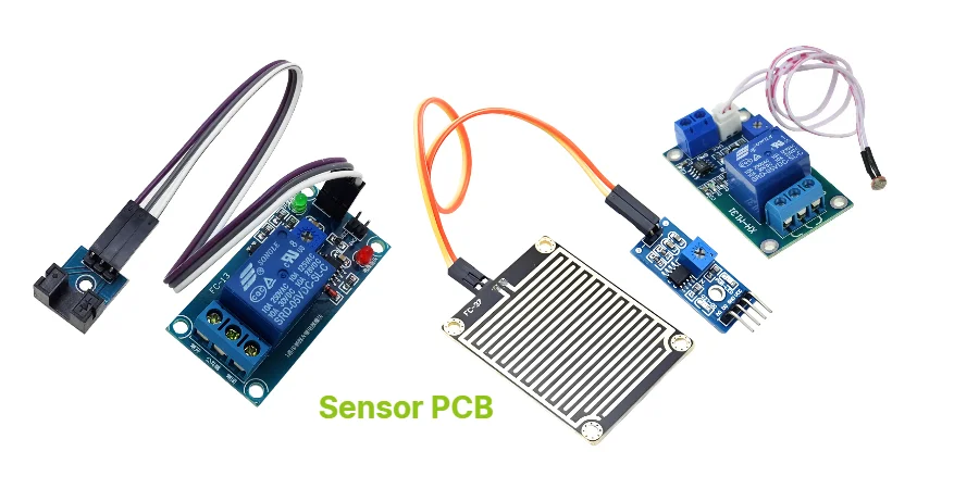
Sensor PCBs are at the heart of modern measurement and control systems, demanding exceptional analog performance, noise immunity, and environmental resilience. Highleap PCB Factory (HILPCB) manufactures and assembles specialized Sensor PCBs for industrial monitoring, automotive safety systems, medical diagnostics, wearable technology, and smart home products. Our manufacturing processes focus on the precise requirements that ensure accurate sensing, long-term stability, and reliable operation in challenging environments.
Sensor PCB Requirements: Precision, Stability, and Integration
Different sensor types present unique PCB challenges—from ultra-low-level analog signals to mixed-signal processing and power control:
Material flexibility: We support standard FR-4 for general applications; high-Tg PCB for harsh thermal environments; ceramic PCB for extreme temperatures; and flex PCB or rigid-flex PCB for space-constrained wearables and dynamic applications.
Signal preservation: Our designs implement continuous ground planes under sensitive traces, star-grounding for analog sections, and domain isolation between digital/power circuits to minimize interference.
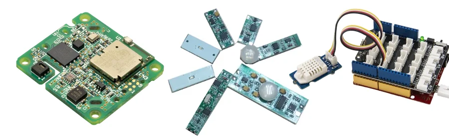
Sensor peripherals: We manufacture complete sensor ecosystems including interface boards, data acquisition cards, wireless sensor PCBs, actuator drivers, and calibration fixtures—all managed within the same ECO system to maintain compatibility.
Design foundation: Begin by mapping the entire measurement chain from sensor through analog front-end to ADC/DSP and interface circuits. Establish noise and drift budgets at each stage, with special attention to reference circuits and return paths.
Material Selection for Precision Sensing Applications
Material selection fundamentally shapes sensor PCB performance across diverse operating conditions and sensing technologies. Standard FR-4 provides an excellent foundation for general sensor applications where temperature ranges remain moderate and environmental stressors are limited. However, many sensing applications push beyond these boundaries, requiring specialized substrate materials. High-Tg PCB materials significantly reduce thermal expansion issues in automotive and industrial sensors that experience wide temperature fluctuations, while providing the stability needed for precise analog measurements over extended operating lifetimes. For extreme environments with temperatures exceeding 150°C or requiring exceptional thermal conductivity, ceramic PCB substrates deliver unmatched dimensional stability and heat dissipation, critical for maintaining calibration in precision measurement systems.
The physical form factor of modern sensor applications frequently demands flexible or hybrid solutions. Wearable medical sensors, implantable devices, and space-constrained consumer products benefit from flex and rigid-flex constructions that enable three-dimensional packaging while maintaining signal integrity. These specialized materials allow sensor designs to conform to curved surfaces, fold into compact enclosures, or connect across moving parts—situations where traditional rigid boards would fail. For power-intensive sensor applications that include excitation sources like heaters, LEDs, or driver circuits, metal-core PCB technology provides superior thermal management by efficiently spreading heat away from critical components, ensuring measurement accuracy isn't compromised by localized temperature gradients.
Stackup architecture plays an equally important role in sensor performance, particularly for low-level signal detection. Optimized stackups place analog layers adjacent to dedicated, quiet reference planes that shield sensitive traces from digital noise. Digital signal routing belongs on separate layers with their own reference planes, with carefully controlled via transitions between domains. When ultra-low-level signals must travel through the stackup, minimizing via transitions or precisely controlling anti-pad and via barrel dimensions becomes crucial to preserving signal integrity. This systematic approach to material selection and stackup design creates a foundation for sensor PCBs that deliver consistent performance under real-world operating conditions.
Layout, Assembly, and Calibration
Precision layout and meticulous assembly are essential for sensor accuracy:
Layout techniques: We implement guard rings around high-impedance nodes, differential sensing topologies where applicable, Kelvin connections for low-resistance measurements, minimized loop areas, and orthogonal routing to prevent signal coupling.
Assembly precision: Our assembly lines carefully handle fine-pitch analog front-ends, delicate MEMS sensors, RF modules, and specialized connectors with controlled temperature profiles for heat-sensitive components.
Calibration and verification: We help establish calibration procedures, test fixtures, and verification steps during development. Production processes include per-lot validation and environmental stress testing as required.
Manufacturing enhancement: Consider conformal coating for dust/humidity protection and underfill for components exposed to mechanical shock. For flexible sensor designs, clearly define bend radii and keep sensitive components away from dynamic flex zones.
Cost, Lead Time, and Documentation Requirements
Successful sensor PCB projects require attention to these key planning factors:
Cost drivers: Stackup complexity, HDI requirements, specialized materials (ceramics/metal-core), calibration/test time, and additional processes like coating or encapsulation.
Typical lead times: Prototypes 7–12 business days; production runs 2–4 weeks depending on material selection and test requirements.
Essential documentation: Sensor orientation references, grounding scheme diagrams, calibration procedures, surface finish specifications, detailed stackups, and acceptance criteria including sensitivity, offset, and drift limits.
For optimal results, review design data with our engineering team and utilize our online tools before finalizing production files.
Why HILPCB for Sensor PCB Projects
Precision manufacturing: We maintain analog signal fidelity and ensure repeatable performance from prototype through volume production.
Material versatility: Our capabilities span standard FR-4, high-Tg PCB, ceramic PCB, and advanced HDI technologies to match your specific environmental and accuracy requirements.
Form factor flexibility: We support compact wearable designs with flex PCB and rigid-flex PCB technologies, and high-power sensing applications with metal-core PCB thermal management.
Frequently Asked Questions
Which materials are best for rugged sensor applications?
For high temperature and vibration environments, consider ceramic PCB or high-Tg PCB. For applications with high-power heating elements or LEDs, metal-core PCB provides superior thermal management. Miniaturized designs benefit from HDI techniques.Can you manufacture flexible sensor PCBs for wearables?
Absolutely—we specialize in flex PCB and rigid-flex PCB technologies for wearable sensors and compact probe applications with carefully defined bend radii and dynamic zones.What techniques protect low-level analog signals in sensor designs?
We implement guard rings, differential signal routing, short return paths, clean reference planes, and minimized via transitions. Our DFM review includes detailed analysis of grounding strategies and potential noise coupling paths.Do you assemble MEMS sensors and fine-pitch analog components?
Yes—our assembly capabilities include precision placement and controlled reflow profiles for sensitive components, with comprehensive AOI, X-ray inspection, and functional testing.What are typical lead times for sensor PCB projects?
Prototypes generally require 7–12 business days; production runs average 2–4 weeks depending on stackup complexity, material selection, and calibration/test requirements.How do you handle sensor calibration and validation?
We integrate calibration procedures according to your specifications and can implement environmental stress testing to verify performance under various conditions. Simply include your acceptance criteria for sensitivity, offset, and drift in the build documentation.What approaches reduce sensor PCB costs while maintaining accuracy?
Focus premium materials only on the areas that directly impact measurement quality, optimize HDI usage, and design with testability in mind. Early collaboration on stackup design and DFM reviews prevents costly re-spins and streamlines calibration processes.