At HILPCB, we design and manufacture advanced power electronics—from automotive motor controllers to high-brightness LED arrays—serving applications where effective thermal management directly determines product lifetime and operational stability. In high-power-density systems, one design factor plays a decisive role in reliability: thermal via architecture.
In real-world validation, even when premium semiconductors, optimized switching algorithms, and sophisticated control systems are in place, a design can fail if heat removal is inadequate. In power modules such as EV inverters, insufficient thermal via density, improper copper plating, or poor alignment to heat-generating components can lead to localized hotspots, triggering thermal runaway, reduced efficiency, and forced power derating.
Robust thermal via design—integrating precise via geometry, copper fill optimization, and stack-up thermal pathways—is essential for maintaining target performance under sustained load conditions. This is where our engineering and manufacturing expertise ensures both thermal efficiency and long-term reliability in demanding environments.
Power Density Evolution: Fighting Physics
Electric vehicle powertrains exemplify the thermal management challenge facing modern electronics. A typical EV inverter must handle 200kW+ of power while fitting into spaces that previously housed much smaller systems. Power density targets of 100W/cubic inch push thermal design to its limits, where every degree of temperature reduction extends component life and improves system efficiency.
The situation becomes even more critical in applications like LED lighting, where thermal management directly affects light output, color stability, and operational lifetime. High-power LEDs can exceed 200W per square inch, requiring sophisticated thermal via arrays to prevent catastrophic thermal runaway that destroys both the LED and surrounding electronics.
Manufacturing Excellence: From Thermal Theory to Practical Solutions
The HILPCB Approach to Thermal Via Implementation
At HILPCB, we've developed systematic thermal design methodologies that transform heat removal requirements from theoretical calculations into manufacturable PCB solutions. This process integrates thermal simulation, materials engineering, and precision manufacturing to achieve optimal thermal performance.
Thermal Simulation and Modeling
Our engineering team employs advanced finite element analysis to predict thermal behavior before committing to fabrication. This isn't basic steady-state analysis—we model transient thermal behavior, including thermal cycling effects and power pulsing scenarios that affect real-world operation.
Critical factors in our thermal modeling include copper distribution optimization, via fill materials and their thermal properties, substrate thermal conductivity variations, and interface thermal resistance at solder joints. Advanced modeling reveals thermal hotspots and enables optimization of via placement for maximum heat removal efficiency.
Precision Manufacturing for Thermal Performance
Achieving effective thermal via performance requires exceptional control over manufacturing variables that affect thermal conduction. Our production systems maintain strict control over:
- Via drill accuracy maintaining ±0.05mm positional tolerance for dense thermal via arrays
- Copper plating thickness ensuring uniform thermal conduction through via barrels
- Via fill consistency using thermally conductive materials to eliminate air gaps
- Surface planarity optimizing thermal interface contact with heat sinks and thermal pads
We don't just rely on standard via processes—our thermal-optimized manufacturing includes specialized techniques like heavy copper plating, thermal via filling with conductive epoxies, and precision surface finishes that optimize thermal interface performance.
Advanced Thermal Via Technologies
Some applications demand thermal management beyond standard capabilities. For these cases, we offer specialized thermal via solutions:
Metal core PCB Integration combines aluminum or copper substrates with strategic thermal via placement to create hybrid thermal management systems. This approach provides exceptional thermal conductivity for applications requiring the ultimate in heat removal performance.
Heavy copper PCB Implementation utilizes copper weights up to 20oz to create low thermal resistance paths that complement thermal via arrays. The combination of heavy copper planes and dense thermal vias provides superior thermal performance for high-power applications.
Embedded Thermal Solutions integrate thermal interface materials directly into the PCB structure, eliminating interface thermal resistance and improving overall system thermal performance. This technique has proven particularly effective for compact power modules and high-density LED arrays.
PCB Substrate Selection for Thermal Applications
Advanced Material Options for Heat Management
- High thermal PCB Materials — Specialized substrates with thermal conductivity 5-10x higher than standard FR4; essential for power electronics requiring maximum heat removal efficiency.
- Ceramic Substrates — Aluminum nitride and aluminum oxide provide exceptional thermal conductivity combined with electrical isolation; ideal for high-voltage power applications requiring reliable insulation.
- Metal Core Laminates — Aluminum or copper cores with dielectric layers enable direct thermal conduction to heat sinks while maintaining electrical isolation between circuits.
Thermal Interface Optimization
Effective thermal via design extends beyond the PCB itself to include thermal interfaces:
- Power semiconductor packages require optimized thermal pad designs that maximize contact area while minimizing thermal resistance through solder joints.
- Heat sink interfaces benefit from smooth surface finishes and thermal interface materials that eliminate air gaps and reduce contact thermal resistance.
- System-level thermal design must consider thermal expansion mismatches that can create stress fractures and degrade thermal performance over temperature cycling.
Testing and Validation: Thermal Performance Verification
Comprehensive Thermal Characterization
Real thermal performance validation requires sophisticated testing that goes beyond simple temperature measurements. Our thermal testing laboratory incorporates multiple verification methods:
Infrared Thermal Imaging: High-resolution thermal cameras map temperature distributions across PCB surfaces with 0.1°C resolution, revealing thermal hotspots and validating heat spreading effectiveness. This technique identifies areas where thermal via density may be insufficient or where thermal interface problems exist.
Thermal Transient Testing: Specialized test equipment characterizes thermal response times and thermal time constants that affect power cycling capability. This data validates thermal via effectiveness under realistic operating conditions including power pulsing and thermal cycling.
Junction Temperature Measurement: Direct measurement of semiconductor junction temperatures during operation validates that thermal via designs maintain safe operating temperatures under maximum power conditions.
Advanced Thermal Analysis Methods
For applications pushing thermal management limits, standard temperature measurements aren't sufficient. We employ sophisticated analysis techniques:
Thermal Resistance Measurement quantifies the effectiveness of thermal via designs by measuring temperature rise per watt of power dissipation. This standardized metric enables comparison between different thermal via configurations and validates design optimization.
Rigid-flex PCB Thermal Analysis addresses the unique challenges of thermal management in flexible assemblies where thermal conduction paths may be interrupted by flex regions. Specialized testing validates thermal performance through mechanical flexing cycles.
Statistical Analysis of thermal test data identifies correlations between manufacturing variations and thermal performance, enabling process optimization for consistent thermal characteristics across production volumes.
Common Pitfalls and How to Avoid Them
Critical Design Errors That Compromise Thermal Performance
Even with advanced manufacturing capabilities, certain design mistakes will sabotage thermal via effectiveness from the start:
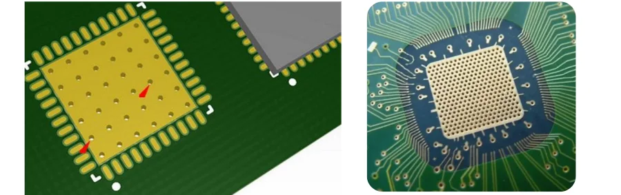
- Insufficient Via Density: Thermal resistance is inversely proportional to the total cross-sectional area of thermal vias. Too few vias create thermal bottlenecks that limit heat removal regardless of other system improvements. Calculate required via density based on power dissipation and target temperature rise.
- Poor Via Placement: Random via placement wastes thermal via effectiveness. Position thermal vias directly under heat sources and create continuous thermal conduction paths to heat removal systems. Avoid placing vias in areas where they don't contribute to heat removal.
- Inadequate Copper Distribution: Thermal vias are only effective when connected to sufficient copper area for heat spreading. Ensure adequate copper planes and thermal pads to collect and distribute heat to thermal via arrays.
Manufacturing Variations to Anticipate
Understanding realistic fabrication tolerances enables better thermal design margins:
- Via Drill Tolerance: ±0.05mm positional accuracy typical; thermal via arrays require precise spacing for optimal thermal performance
- Copper Plating Thickness: ±20% variation affects thermal conduction; specify minimum plating thickness for thermal applications
- Via Fill Quality: Air voids in via fill reduce thermal conductivity; specify thermal via fill materials and inspection criteria
- Surface Planarity: ±25μm surface variation affects thermal interface contact; specify surface finish requirements for thermal interfaces
Design Tip: Model manufacturing tolerances in thermal simulations and include safety margins to ensure adequate thermal performance across production variations.
Partner with HILPCB for Thermal Excellence
Successful thermal via design requires more than manufacturing capability—it demands deep understanding of heat transfer physics, materials science, and practical thermal management constraints. At HILPCB, we combine thermal engineering expertise with proven manufacturing experience to deliver consistent, reliable thermal performance for your most demanding power applications.
Our commitment extends beyond meeting thermal specifications. We partner with you throughout the design process, offering:
- Thermal simulation and optimization to ensure manufacturable thermal solutions
- Material selection guidance based on your specific power density and environmental requirements
- Prototype validation with comprehensive thermal testing and performance documentation
- Volume production with statistical process control and thermal performance monitoring
- Failure analysis and thermal design optimization when challenges arise
Whether you're designing next-generation electric vehicle powertrains, high-efficiency LED lighting systems, or compact power supplies, effective thermal via design can make the difference between market success and thermal failure. Don't leave thermal management to chance.