
Heavy Copper PCB Manufacturer | 3–20 oz Power Circuit Boards | Quickturn
Direct factory heavy copper PCB manufacturer specializing in 3 oz to 20 oz thick copper boards. Among specialized heavy copper pcb manufacturers, HilPCB delivers 24–48h rapid prototyping for 2–6 oz copper, competitive tiered volume production pricing, and 100% automated electrical testing.
Capabilities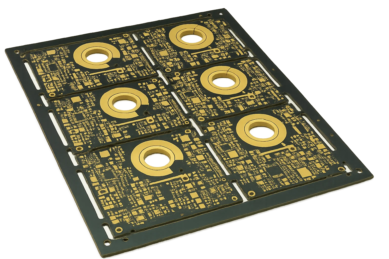
Heavy Copper Engineering & Cost Optimization
Strategic implementation for current density and thermal balanceHeavy copper PCBs are justified when trace currents exceed ~30–50 A or when integrated thermal paths are required without external bus bars. Typical applications include power converters, automotive inverters, and industrial drives. We evaluate copper weight selection (3–6 oz commonly sufficient; 10 oz or more for high-power stages), thermal spreading (temperature rise reduction of 10–30 °C), and manufacturing trade-offs such as plating uniformity and layer stress. Through systematic power distribution optimization, heavy copper boards can eliminate bus bars and reduce assembly steps by 40–60%.
Current capacity follows IPC-2152 guidance with derating for ambient temperature, adjacent heat sources and enclosure constraints. For example, a 4 oz copper trace at 10 mm width can carry approximately 50–80 A with moderate temperature rise — actual limits depend on copper thickness, trace geometry and airflow conditions. While moving from 2 oz to heavy copper may increase PCB cost by 25–40%, total system cost often drops due to fewer interconnects and improved heat dissipation.
Critical Risk: High current density and poor plating uniformity can cause localized heating, delamination, or inner-layer etch imbalance. Excessive copper thickness without proper copper balancing can warp panels during lamination or create drill breakout during fabrication.
Our Solution: We apply advanced current density modeling and differential plating control to achieve uniform copper distribution across layers. Thermal vias and metal core PCBs are integrated where heat spreading is critical. Stackups follow IPC-6012 Class 3 reliability standards with X-ray verification of via fill and plating CPK ≥ 1.33. For optimized thermal and electrical co-design, see our thermal design guidelines and high-thermal PCBs.
- Copper thickness 105–700 μm = 3–20 oz
- Current capacity modeled to IPC-2152 with environment-specific derating
- Thermal via arrays Ø0.30–0.50 mm for heat extraction
- Differential etching compensation for mixed copper weights
- Temperature rise control via copper spreading: ΔT 10–30 °C
- Hybrid stackups combining power layers with standard control circuitry
🚀 Quick Quote Request
📋 Get Full Capabilities
Plating Uniformity & Differential Etching Process Control
Multi-stage manufacturing for thickness consistency and adhesionExtended electroplating for heavy copper (e.g., ~4–8 h — for 10 oz buildup) uses controlled current density and pulse-reverse profiles to maintain uniformity within ±10%. Step-down etching recipes address undercut; lateral etch can approach a 1:1 ratio with copper thickness at extreme weights, so mask/chemistry timing is carefully staged. High-Tg materials 170–180 °C withstand multiple reflows and prolonged plating exposure.
Our extreme copper processing integrates AOI at multiple stages, cross-sections for adhesion, and high-current load testing with IR thermography to validate thermal models. Warpage is held ≤0.75% on typical panels via pressure-profiled lamination. See our assembly quote guide for schedule/cost levers.
- Computer-controlled plating with thickness mapping at 25 points
- Step-down etching for fine features near heavy copper
- High-pressure lamination up to ~500 psi
- Thermal shock −40 °C↔+125 °C for automotive profiles
Heavy Copper PCB Capability & Performance Matrix
Process windows for high-current power distribution
| Parameter | Standard Capability | Advanced Capability | Standard |
|---|---|---|---|
Layer Count | 2–8 layers | Up to 32 layers | IPC-2221 |
Base Materials | FR-4 high-Tg 170–180 °C | High thermal conductivity FR-4, Rogers, Metal Core (IMS) | IPC-4101 |
Board Thickness | 1.6–3.2 mm | 0.8–8.0 mm | IPC-A-600 |
Copper Weight | 3–6 oz (105–210 μm) | Up to 20 oz (700 μm) | IPC-4562 |
Min Trace/Space | 150/150 μm (6/6 mil) | 100/100 μm (4/4 mil) | IPC-2221 |
Min Hole Size | 0.30 mm (12 mil) | 0.20 mm (8 mil) | IPC-2222 |
Via Technology | Through-hole, Thermal vias | Copper-filled vias, Press-fit, Blind/Buried | IPC-6012 |
Max Panel Size | 571.5 × 609.6 mm | 571.5 × 1200 mm | Manufacturing capability |
Current Capacity | Up to ~100 A per trace (design dependent) | 200 A+ (design dependent) | IPC-2152 |
Surface Finish | HASL lead-free, ENIG, OSP | Immersion Silver, ENEPIG, Hard/Thick Gold | IPC-4552/4556 |
Quality Testing | E-test, AOI, Cross-section | High-current load, Thermal shock, IR thermography | IPC-9252 / IPC-TM-650 |
Certifications | ISO 9001, UL, RoHS | IATF 16949, AS9100, IPC-A-610 Class 3 | Industry standards |
Lead Time | 7–10 days | ≈5 days (complexity dependent) | Production schedule |
Ready to start your PCB project?
Whether you need simple prototypes or complex production runs, our advanced manufacturing capabilities ensure excellent quality and reliability. Get your quote within 30 minutes.
Thermal Design Integration & Current Distribution Strategy
Go beyond simple current tables: size traces per IPC-2152 then validate with boundary conditions (ambient, airflow, enclosure). For continuous duty, many designs cap ΔT near 10–20 °C, with transients up to 30–40 °C. Large copper planes dissipate ~3–5× heat compared to isolated traces of equal cross-section.
Thermal vias: Ø0.30–0.50 mm at 1.0–1.5 mm pitch beneath hot devices. Copper-filled vias can increase vertical conductivity by ~10–20×. Create direct paths to spreading layers or heatsinks. See thermal via design.
Mixed copper weights require stackup planning to avoid resin starvation and thickness steps. Placing 3–6 oz power layers near the outside improves heat shedding; inner 1–2 oz layers handle control signals. This hybrid approach can reduce material cost by 20–30% while meeting current targets.
Need Expert Design Review?
Our engineering team provides free DFM analysis and optimization recommendations
Heavy Copper PCB for Thermal Management and High Current Distribution
A heavy copper PCB for thermal management does two jobs at once: it carries large current with acceptable resistive loss, and it spreads heat away from the devices that generate it. Those goals can conflict, because the copper that lowers resistance also conducts heat into the substrate, and the laminate decides how much of that heat can leave through the base.
Sizing for high current. A high-current heavy copper PCB is not dimensioned by nominal ampacity alone. Trace width, copper weight, ambient temperature, allowable temperature rise and the presence of plane copper all interact. Published ampacity charts assume still air and a single isolated conductor, so use them as a starting point and confirm with a thermal measurement on a representative coupon. Where current is extremely high, parallel layers or busbar construction may be more effective than adding copper weight.
Copper weights and what they mean. Designs commonly specify 4 oz, 6 oz or 8 oz copper depending on the current and thermal path. Above roughly 3 oz, etching behaviour changes: sidewalls become sloped, minimum line width and spacing widen, and the achievable feature density drops. Those constraints must be reflected in the design rules before layout, not discovered during fabrication.
Thickness uniformity and reliability. Copper thickness uniformity is one of the strongest predictors of yield, because plating variation changes both resistance and the dielectric gap. Processes that rely on heavy plating must control distribution across the panel. A thermal reliability program then verifies the result through thermal cycling and microsection, since thick copper and thick dielectric expand at different rates under load.
For automotive and industrial programs the same part must satisfy automotive durability expectations, which means documented process control rather than a one-off sample result. See the high thermal PCB options when substrate conductivity is the limiting factor.
Sequential Processing & Quality Control Methodology
Base foil (35–70 μm) influences adhesion and final morphology. Plating deposition ~25–30 μm/h preserves grain structure. Hull-cell and coupon mapping tune current density. Photoresist thickness scales with copper weight (e.g., 75–100 μm for ~10 oz) to survive longer etch times; regenerative etch maintains stable copper loading. Differential etch achieves 100–150 μm features beside heavy copper. Acceptance aligns to IPC Class 3 microsection criteria.
Lamination: staged ramps to ~185 °C and pressures up to ~500 psi prevent voids. Dimensional stability holds ±0.10 mm per 300 mm. Assembly for heavy copper pads may require preheat and extended reflow soak to ensure wetting.
Substrate Selection for Thermal & Electrical Performance
Choose materials by thermal conductivity, Tg and z-axis CTE. FR-4 high-Tg 170–180 °C supports moderate rises (<40–50 °C). For higher loads, filled systems offer 0.6–1.0 W/m·K, ~2–3× standard FR-4. For extreme dissipation, IMS (metal core) provides 1.0–8.0 W/m·K but limits layer count; see metal core PCB.
Hybrid stackups with thermally conductive prepregs (0.5–0.7 W/m·K) between power layers, plus standard materials for signal layers, can cut costs by 30–40% while preserving thermal performance. Qualify with delamination after multiple reflows and CAF resistance for high-voltage paths.
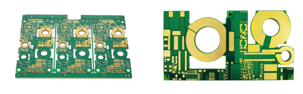
Reliability Testing Matrix & Performance Validation
High-current load tests apply 50–200 A while IR thermography confirms steady-state temperature and absence of hot spots (>10 °C). Endurance runs can last 4–8 h, with automotive profiles requiring up to 100 h.
Thermal cycling: −40 °C to +125 °C with 15-minute dwells for 500–1000 cycles. Accept if ΔR ≤10%. Cross-sections review barrel cracks and adhesion. See thermal reliability testing.
Mechanical: PTH pull strength targets >8 lbf for Ø0.80 mm holes; assembly profiles extend soak for 6–10 oz pads to ensure wetting. Full traceability covers materials, process parameters and test data for each lot.
Application-Specific Heavy Copper Implementation
EV power electronics/BMS: 6–10 oz main buses for 200–400 A continuous with junction-to-coolant θJB <0.5 °C/W.
Industrial drives/welding: 10–20 oz for peaks >300 A, distributed thermal vias (50–100 per TO-247) for >100 W/cm².
Renewables: selective heavy copper only on high-current paths to balance cost vs lifetime reliability.
Heavy Copper PCB Cost, Quality Control and Prototype Planning
Buyers often ask how to make a heavy copper PCB cost-effective without compromising the current path. The honest answer is that cost is driven by process yield, and yield on thick copper is dominated by a few design choices rather than by copper price itself.
What drives cost. Extremely wide traces, very tight spacing at high copper weight, and multiple sequential lamination cycles are the main cost multipliers. Allowing generous spacing at heavy copper, consolidating layers, and keeping heavy copper out of the fine-pitch regions (using a hybrid or partial-thickness approach where possible) usually reduces cost more than negotiating piece price. A heavy copper prototype run is the correct place to prove these trade-offs before committing tooling and panels.
Quality control that matters. Effective quality control on a heavy copper build focuses on the parameters that vary at high copper: plated thickness distribution, etch compensation, dielectric thickness over heavy features, and lamination voiding at thick-to-thin transitions. Microsection at representative locations plus electrical verification of the power nets catches the failures that visual inspection misses. Where the board must survive aerospace or defence program review, that evidence has to be lot-specific.
Thermal and market context. Demand for heavy copper boards has grown with electrification, and applications now span EV power stages, industrial drives, renewable inverters and high-power LED systems. Each has different acceptance criteria: automotive programs weight thermal cycling and traceability, industrial programs weight long-term supply stability, and aerospace work adds qualification documentation on top. Open with the program context in the quote request, since it changes both stackup and evidence package.
Engineering Assurance & Certifications
Experience: production-proven heavy copper and extreme copper builds with zone-controlled lamination and staged etch.
Expertise: IPC-2152 modeling + IR validation; SPC on plating/etch; Cpk targets ≥1.33.
Authoritativeness: IPC Class 3, IATF 16949, ISO 13485, AS9100; audit-ready documentation.
Trustworthiness: MES ties lot codes/serialization to in-line test data; thermal/load reports available.
- Process controls: plating thickness, etch undercut, lamination pressure/temperature
- Traceability: unit serialization, component lot tracking, digital traveler
- Validation: load tests, thermal cycling/ shock, microsections per IPC-TM-650
Frequently Asked Questions
What copper thickness qualifies as heavy vs extreme copper?
How do thermal vias and planes work together?
Which factory controls matter most for reliability?
When should I specify IMS or metal core instead of FR-4 heavy copper?
Does heavy copper affect assembly?
How is copper weight chosen for high current heavy copper PCBs?
Experience Advanced PCB Manufacturing Excellence
From simple prototypes to complex production runs, our world-class factory delivers superior quality, fast turnaround and competitive pricing. Join thousands of satisfied customers who trust us with their PCB manufacturing needs.