
High Thermal Conductivity PCB | Metal Core (MCPCB) & Ceramic | Power and LED Thermal Design
Thermal-path engineered PCBs for LEDs and power electronics: aluminum/copper MCPCB, alumina/aluminum-nitride ceramic, heavy copper planes, and high-density thermal vias. Verified −40↔+125 °C cycling and flatness control for optimal TIM contact.
Capabilities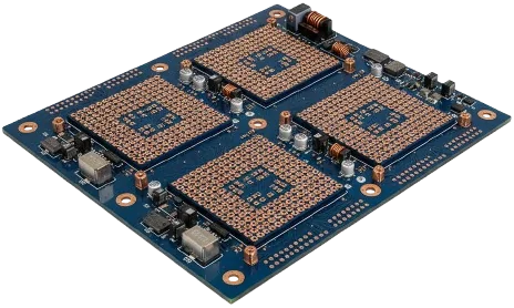
Thermal Path Engineering & Material Selection
Optimize junction-to-ambient resistance from source to sinkWhen power density exceeds ~0.5–1.0 W/cm² or junction temperatures approach device limits, the PCB itself must act as an active heat spreader. Standard FR-4 PCB offers ~0.3–0.4 W/m·K of thermal conductivity, insufficient for high-power or LED applications. To bridge this gap, we deploy three core approaches: metal core PCBs (MCPCBs) for cost-effective LED and power boards, ceramic PCBs (Al₂O₃ or AlN) for CTE-matched and high-conductivity designs, and heavy copper PCBs to enhance lateral heat spreading beneath power semiconductors and MOSFETs.
In MCPCB stackups, the dielectric layer—typically 75–150 μm—dominates total thermal resistance. Optimizing resin type and filler ratio can reduce it by 20–30%. Thermal-via arrays positioned under heat sources further lower vertical resistance paths. See our MCPCB design guidelines and LED PCB manufacturing guide for detailed stackup and layout strategies.
Critical Risk: Insufficient heat dissipation leads to junction temperature runaway, solder joint fatigue, or delamination due to repeated thermal cycling. Inconsistent dielectric thickness or poor via fill also increases thermal impedance, reducing device lifetime by up to 40%.
Our Solution: We apply thermal shock and cycling validation from −40 °C to +150 °C to verify material stability and interface adhesion. Using FEA-based (Finite Element Analysis) thermal simulation, we model hot-spot spreading and optimize copper distribution, dielectric formulation, and via patterning for consistent heat flow. For extreme cases, ceramic PCBs or high-Tg PCBs are recommended to combine thermal stability with mechanical strength.
For additional insight into system-level reliability, explore our PCB thermal management blog and related high-thermal PCB case studies to see proven design approaches for LED lighting, EV converters, and industrial power electronics.
- MCPCB system conductivity typically 1–3 W/m·K
- Ceramic options: Alumina ~18–25 W/m·K; AlN ~150–170 W/m·K
- Thermal via arrays: Ø0.30–0.50 mm, 1.0–1.5 mm pitch
- Heavy copper ≥3 oz for spreading
- CTE-aware footprints to protect solder joints during cycling
🚀 Quick Quote Request
📋 Get Full Capabilities
Controlled Processes for Repeatable Thermal Performance
Void-free bonding, thickness tolerance and surface planarityVacuum lamination bonds thin, ceramic-filled dielectrics to metal cores with thickness control ±10% to stabilize thermal resistance. For ceramic PCB, DBC/DPC interfaces are validated by thermal shock and microsection analysis. Copper-filled vias improve vertical conduction by ~10–20× over resin-filled designs. Our thermal reliability testing covers −40↔+125 °C to secure interface integrity.
Mounting-surface planarity and roughness drive TIM effectiveness: we hold Ra ≤3 μm and local flatness within ±25 μm over pad fields. Where high current and heat coexist, combine MCPCB or ceramic modules with heavy copper distribution layers for robust PDN and cooling.
- Vacuum lamination to eliminate voids in dielectric
- Dielectric thickness tolerance ±10%
- Copper-filled thermal vias (10–20× conductivity vs. resin-filled)
- Surface flatness/windows tuned for TIM performance
- Automotive cycling −40↔+125 °C
Thermal PCB Technical Capabilities
Engineered for LEDs, power conversion and RF PA modules
| Parameter | Standard Capability | Advanced Capability | Standard |
|---|---|---|---|
Layer Count | 1–4 layers MCPCB | Up to 40+ layers thermal FR-4 hybrids | IPC-2221 |
Base Materials | Aluminum MCPCB, thermal FR-4 | Copper core MCPCB, ceramic (Alumina, AlN) | IPC-4101/4103 |
Thermal Conductivity (system) | 1–3 W/m·K | 5–20 W/m·K (material dependent) | ASTM E1461 |
Dielectric Thickness (MCPCB) | 75–150 μm | ≤50 μm high-performance dielectric | Manufacturer datasheet |
Board Thickness | 0.8–3.2 mm | 0.4–6.0 mm | IPC-A-600 |
Copper Weight | 1–4 oz | Up to 10 oz | IPC-4562 |
Min Trace/Space | 100/100 μm (4/4 mil) | 75/75 μm (3/3 mil) | IPC-2221 |
Min Hole Size | 0.20 mm (8 mil) | 0.15 mm (6 mil) | IPC-2222 |
Via Technology | Resin-filled thermal vias | Copper-filled vias, stacked microvias | IPC-6012 |
Max Panel Size | 571.5 × 609.6 mm | 571.5 × 1200 mm | Manufacturing capability |
Surface Finish | HASL lead-free, OSP, ENIG | ENEPIG, Immersion Silver, TIM pre-apply | IPC-4552/4556 |
Quality Testing | E-test, thermal stress | Thermal cycling, IR imaging, thermal resistance test | IPC-9252 |
Certifications | ISO 9001, UL, RoHS/REACH | IATF 16949, ISO 13485 | Industry standards |
Lead Time | 5–10 days | 3–5 days expedited | Production schedule |
Ready to start your PCB project?
Whether you need simple prototypes or complex production runs, our advanced manufacturing capabilities ensure excellent quality and reliability. Get your quote within 30 minutes.
Layout Rules: Spreading, Vias and Isolation
Use copper-spreading planes under heat sources and stitch to dense via arrays. Typical thermal-via densities run 50–100 vias/cm² with 0.30–0.50 mm diameters and 1.0–1.5 mm pitch. Keep sensitive analog/RF isolated with thermal cutouts and consider ceramic sub-modules for RF PAs—see ceramic PCB.
Surface quality drives TIM performance: deviations >50 μm across pad fields can raise interface resistance by 20–30%. For estimating cost and schedule trade-offs, review our assembly quote guide.
Need Expert Design Review?
Our engineering team provides free DFM analysis and optimization recommendations
Process Flow: MCPCB and Ceramic
MCPCB: substrate prep → vacuum lamination of ceramic-filled dielectric → circuit etch → drill/plate vias (copper-fill as required) → planarize → finish. Ceramic DBC/DPC: bond copper to ceramic at high temperature, then pattern, drill/laser, and plate. Quality checkpoints include dielectric thickness mapping, void inspection and Ra/flatness metrology. Learn more in thermal shock testing and LED manufacturing articles.
Choosing the Right Substrate
Aluminum MCPCB: balanced cost/performance for LEDs and moderate power.
Copper core: highest spreading and conductivity (base ~380–400 W/m·K), with weight/cost trade-offs.
Alumina (Al₂O₃): 18–25 W/m·K; AlN: 150–170 W/m·K with good CTE match.
Thermal FR-4: 1.0–2.0 W/m·K upgrade path without full redesign. For mixed high-current/high-speed backplanes, see backplane PCB.
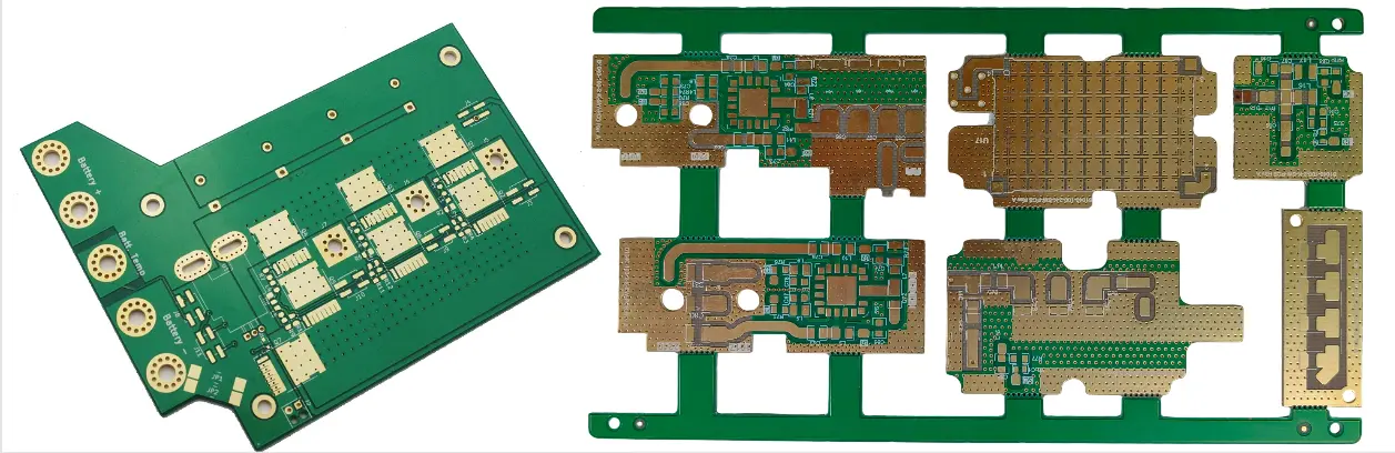
Thermal Characterization & Reliability
We validate Rth (thermal resistance) against design within ±15% using calibrated fixtures; IR thermography confirms uniform heat distribution. Reliability includes power cycling, 85 °C/85% RH moisture stress, and −40↔+125 °C thermal cycling with microsections after stress—see IPC Class 3 manufacturing checks.
LED, Power Conversion and Telecom
LED lighting: street/automotive lamps often target <1 °C/W junction-to-sink paths using aluminum MCPCB.
Power conversion: motor drives, inverters and EV chargers benefit from copper-filled vias and heavy copper planes.
Telecom RF: ceramic substrates support RF PAs with both thermal and dielectric performance. For flexible interconnects near hot zones, pair modules with flex PCB jumpers.
Engineering Assurance & Certifications
Experience: volume LED and power programs using aluminum/copper MCPCB and AlN ceramic.
Expertise: void-free bonding, copper-filled vias, flatness/roughness metrology, and SPC on dielectric thickness and registration.
Authoritativeness: IPC-6012 Class 2/3, IATF 16949, ISO 13485; audit-ready documentation.
Trustworthiness: MES connects supplier lots, serialization and thermal-test data; lot reports available.
- Controls: dielectric thickness ±10%, Ra ≤3 μm, flatness ±25 μm
- Traceability: lot codes, unit-level serialization, digital traveler
- Validation: thermal cycling, IR imaging, microsections
Frequently Asked Questions
MCPCB vs ceramic vs thermal FR-4: how should I choose?
How many thermal vias do I need under a power device?
Can thermal PCBs remove the need for a heat sink?
Which surface finish is best for thermal interfaces?
How do you verify thermal performance in production?
Experience Advanced PCB Manufacturing Excellence
From simple prototypes to complex production runs, our world-class factory delivers superior quality, fast turnaround and competitive pricing. Join thousands of satisfied customers who trust us with their PCB manufacturing needs.