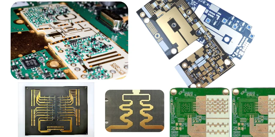
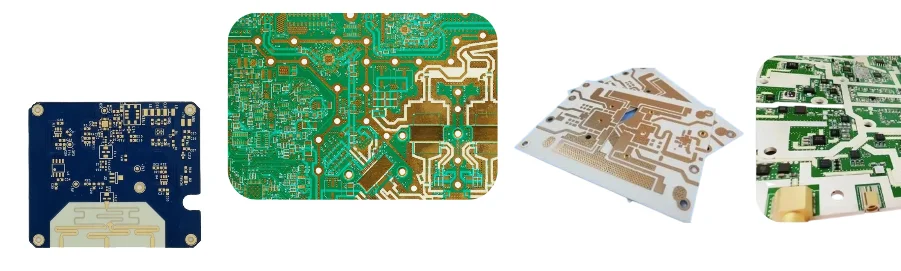
In today's interconnected world of 5G networks, satellite communications, and automotive radar systems, high-frequency PCB technology has become the backbone of modern electronics. HF PCB, or High-Frequency Printed Circuit Board, represents a specialized category of circuit boards designed to operate reliably at frequencies ranging from hundreds of megahertz to over 100 gigahertz. This comprehensive guide explores what makes HF PCBs unique, their critical applications, and why choosing the right high-frequency solution is essential for your next RF or high-speed digital project.
1. Understanding HF PCB: Definition and Frequency Ranges
HF PCB refers to printed circuit boards specifically engineered to handle high-frequency signals with minimal loss, distortion, and interference. Unlike standard PCBs that work well for DC and low-frequency applications, HF PCBs require specialized materials, precise manufacturing processes, and careful design considerations to maintain signal integrity at elevated frequencies.
The term "high-frequency" in PCB context typically encompasses several frequency bands:
- RF Band (1 MHz - 1 GHz): Used in radio communications, RFID, and wireless sensors
- Microwave Band (1 GHz - 30 GHz): Essential for cellular networks, WiFi, and satellite communications
- Millimeter Wave (30 GHz - 300 GHz): Critical for 5G networks, automotive radar, and advanced imaging systems
- Sub-THz (>100 GHz): Emerging applications in 6G research and scientific instruments
At these frequencies, PCB traces no longer behave as simple conductors but become transmission lines where every geometric detail affects signal propagation. A trace carrying a 10 GHz signal on a standard FR4 substrate experiences approximately 1.5 dB/inch of loss, making material selection and design optimization crucial for maintaining signal quality.
2. Key Characteristics That Define HF PCBs
What distinguishes HF PCBs from conventional circuit boards are several critical characteristics that enable reliable high-frequency operation. Understanding these properties is essential for anyone working with RF, microwave, or high-speed digital systems.
Low Dielectric Constant (Dk) and Loss Tangent (Df)
The dielectric constant determines how fast signals propagate through the PCB substrate, while loss tangent indicates how much signal energy is absorbed. HF PCBs utilize materials with:
- Stable Dk values: Typically 2.2-3.5 for optimal performance
- Low Df values: Below 0.005 at operating frequency
- Minimal variation: Dk tolerance within ±0.05 across production batches
- Temperature stability: TCDk less than 50 ppm/°C
Controlled Impedance Requirements
Signal integrity at high frequencies demands precise impedance control:
- Tolerance levels: ±5% for critical applications, ±10% standard
- Consistency: Uniform impedance across trace length
- Matched transitions: Careful via and connector design
- Testing verification: 100% TDR testing for production
Superior Thermal Management
High-frequency circuits often dissipate significant power:
- Thermal conductivity: Enhanced materials (>0.5 W/m·K)
- CTE matching: Reduced stress on solder joints
- Heat dissipation: Thermal vias and copper planes
- Operating range: -55°C to +150°C for automotive applications
3. HF PCB Materials: The Foundation of Performance
The choice of substrate material fundamentally determines HF PCB performance. Unlike standard FR4 which exhibits excessive losses above 1 GHz, specialized high-frequency materials maintain signal integrity across wide frequency ranges.
PTFE-Based Materials
PTFE (Polytetrafluoroethylene) composites offer the lowest loss and most stable electrical properties:
Rogers RT/duroid Series:
- RT/duroid 5880: Dk=2.20, Df=0.0009 at 10 GHz
- RT/duroid 6002: Dk=2.94, Df=0.0012 at 10 GHz
- Applications: Satellite communications, military radar
- Cost: 8-12× standard FR4
Ceramic-Filled Hydrocarbon Materials
These materials balance performance with manufacturability:
Rogers RO4000 Series:
- RO4003C: Dk=3.38, Df=0.0027 at 10 GHz
- RO4350B: Dk=3.48, Df=0.0037 at 10 GHz
- Processing: Compatible with standard multilayer PCB fabrication
- Cost: 3-5× standard FR4
Advanced Thermoset Materials
For high-speed PCB applications requiring moderate RF performance:
Isola I-Tera MT40:
- Dk=3.45, Df=0.0031 at 10 GHz
- Excellent for mixed digital/RF designs
- Lead-free assembly compatible
- Cost: 2-3× standard FR4
4. Critical Applications of HF PCB Technology
HF PCBs enable the wireless and high-speed technologies that define modern life. From smartphones to autonomous vehicles, these specialized circuit boards make advanced electronics possible.
5G and Telecommunications Infrastructure
The rollout of 5G networks relies heavily on HF PCB technology:
- Massive MIMO Base Stations: 64-256 antenna elements requiring precise phase matching
- Small Cell Deployments: Compact designs operating at 28/39 GHz
- Beamforming Arrays: Dynamic beam steering for improved coverage
- Backhaul Links: Point-to-point microwave connections
Technical requirements include:
- Insertion loss <0.5 dB/inch at 28 GHz
- Phase stability ±5° across temperature
- Impedance control ±3%
- Multi-layer constructions up to 20 layers
Automotive Radar Systems
Modern vehicles incorporate multiple radar systems for safety:
- 77 GHz Long-Range Radar: Adaptive cruise control, collision avoidance
- 24 GHz Short-Range Radar: Blind spot detection, parking assistance
- Imaging Radar: 4D environmental mapping for autonomous driving
Automotive HF PCBs must meet:
- AEC-Q100 qualification standards
- -40°C to +150°C operation
- Vibration resistance to 50G
- 15-year reliability targets
Satellite and Aerospace Communications
Space applications demand ultimate reliability:
- LEO Satellite Constellations: Phased arrays for global internet
- Ground Station Equipment: High-gain tracking antennas
- Avionics Systems: Navigation and communication
- Defense Electronics: Radar and electronic warfare
5. Design Considerations for HF PCB Success
Designing HF PCBs requires specialized knowledge and attention to details that can be ignored in low-frequency designs. Every aspect from stackup planning to component placement affects high-frequency performance.
Transmission Line Design
At high frequencies, traces become transmission lines requiring careful design:
Microstrip Configuration:
- Exposed trace on outer layer
- Easier to tune and probe
- Higher radiation and crosstalk
- Typical impedance: 50Ω ±5%
Stripline Configuration:
- Embedded between ground planes
- Superior isolation and shielding
- No dispersion effects
- More complex manufacturing
Via Optimization
Vias represent discontinuities that degrade signal integrity:
- Minimize transitions: Route critical signals on single layer
- Back-drilling: Remove unused via stubs above 5 GHz
- Via fencing: Shield sensitive signals with ground vias
- Blind/buried vias: HDI PCB technology for dense designs
Grounding and Shielding Strategies
Proper grounding ensures stable operation:
- Continuous ground planes: No splits under RF traces
- Stitching vias: Connect ground layers every λ/20
- Edge plating: Reduce edge radiation
- Compartment shielding: Isolate different frequency sections
6. Why Choose HILPCB for Your HF PCB Requirements
HILPCB combines advanced manufacturing capabilities with deep RF expertise to deliver superior high-frequency PCB solutions:
- Comprehensive Material Selection: Full inventory of Rogers, Taconic, Isola, and Arlon materials
- Precision Manufacturing: ±3% impedance control, ±25μm registration accuracy
- Advanced Processes: Sequential lamination, back-drilling, cavity structures
- Testing Capabilities: Network analyzer testing to 67 GHz, TDR verification
- Quick Turnaround: 24-hour quotes, 5-day prototypes
- Technical Support: RF engineers for design consultation and optimization
Our HF PCB manufacturing serves diverse industries including telecommunications, automotive, aerospace, defense, and medical equipment.