
High-Frequency PCB Manufacturing | RF & Microwave PCBs | HilPCB
High-frequency PCB manufacturing for RF, microwave and mmWave designs, with low-loss laminates, hybrid stackups, controlled impedance and file-reviewed testing.
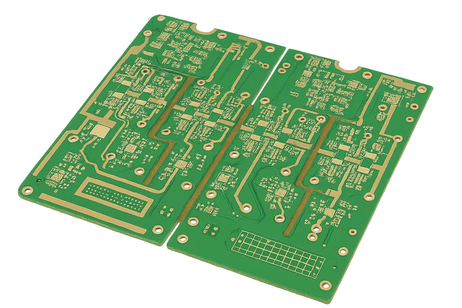
High-Frequency PCB Material Selection for RF Loss Budgets
Dk, Df, copper profile, thickness and availability must be evaluated togetherA high-frequency PCB should not be specified by laminate brand or operating frequency alone. Trace length, insertion-loss budget, phase stability, thermal exposure, copper roughness, board thickness and supply continuity all affect the right material choice. HilPCB reviews these inputs before recommending a low-loss FR-4, hydrocarbon ceramic, PTFE or hybrid construction.
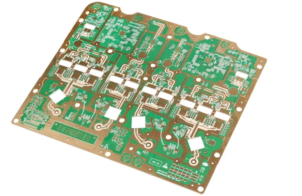
For cost-sensitive designs, a hybrid RF / FR-4 stackup can reserve premium laminate for critical signal layers while using conventional materials elsewhere. Feasibility depends on resin flow, bonding system, copper balance and coefficient-of-expansion compatibility, so the construction is confirmed after stackup and fabrication-file review. Compare common options in our high-frequency PCB materials guide, or review our dedicated Rogers PCB manufacturing service.
Material datasheet Dk and Df values are reference conditions, not automatic finished-board guarantees. The quotation records the proposed material, construction, controlled features and any required coupon or report so procurement and engineering teams are working from the same scope.
- Low-loss FR-4, hydrocarbon ceramic, PTFE and other RF laminate review
- Hybrid RF / FR-4 stackup feasibility assessment
- Datasheet Dk and Df conditions checked against the design model
- Copper profile and surface-finish trade-off review
- Material availability and approved-substitute discussion
- Prototype construction documented for repeat orders
🚀 Quick Quote Request
📋 Get Full Capabilities
High-Frequency PCB Manufacturing Review Before RFQ
Resolve stackup, impedance, via and test requirements before fabricationRF PCB manufacturability depends on the relationship between material behavior and geometry. We review dielectric thickness, copper weight and profile, finished trace geometry, plated-hole structure, lamination sequence, registration demand and surface finish before confirming the build. PTFE and other specialized laminates may require dedicated surface preparation, drilling and bonding controls.
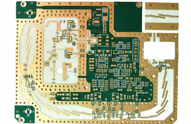
Back-drilling, blind or buried vias, cavity routing and edge plating are evaluated from the actual drill and mechanical data. The same review defines whether impedance coupons, TDR measurements, microsections, electrical test or VNA-related deliverables belong in the order. See the high-frequency PCB manufacturing guide for the process decisions behind a repeatable prototype-to-production handoff.
After review, the quotation identifies what is included, what remains a design target and what requires a separate test method, fixture or acceptance limit. This prevents a supplier datasheet value from being mistaken for a finished-board acceptance criterion.
- Gerber or ODB++, drill data and fabrication drawing review
- Stackup, impedance table and reference-plane consistency check
- Back-drill, blind-via and cavity feasibility review
- Surface finish selected for RF, assembly and storage needs
- Coupon and measurement scope defined before order release
- Open technical questions returned with the quotation
High-Frequency PCB Build and Quote Options
Capabilities are confirmed against the material system, geometry, test scope and order quantity
| Decision Area | Options We Review | What Determines the Quote | Confirmation Basis |
|---|---|---|---|
RF Materials | Low-loss FR-4 and hydrocarbon ceramic laminates | PTFE, ceramic-filled and customer-specified RF laminates | Supplier datasheet / IPC-4103 |
Construction | Single-material RF stackup | Hybrid RF / FR-4 or mixed-laminate stackup | Approved stackup |
Layer Count & Thickness | Up to 60+ layers; finished thickness defined by the fabrication drawing | Multilayer and sequential constructions reviewed case by case | Approved stackup and fabrication drawing |
Copper Profile | Standard or low-profile copper by material availability | Very-low-profile copper when the loss model requires it | Material construction |
Trace / Space | Down to 2/2 mil (50 μm) on eligible constructions | Finished copper, etch compensation, dielectric thickness and RF geometry reviewed together | Finished geometry and process confirmation |
Controlled Impedance | ±5% impedance coupons when the stackup and acceptance method are approved | Target, tolerance, coupon and TDR scope set in the purchase specification | Impedance table, coupon and acceptance method |
Via Structures | Plated through holes | Back-drilled, blind, buried or sequential vias after review | Drill and stackup data |
Surface Finish | ENIG, immersion silver, OSP or other specified finish | Bonding or RF-sensitive finish evaluated by application | Assembly and RF requirements |
Production Test | Electrical test and visual inspection | TDR, microsection or other agreed measurements | Order-specific test plan |
RF Frequency & VNA | 1–67 GHz application review by material and test plan | VNA/S-parameter options above 40 GHz when the test band, fixture and calibration are defined | Test band, fixture and order-specific test plan |
Panel Size & RF Format | Panels up to 500 × 500 mm by panel and RF-format review | Panelization, edge clearance, cavity and launch constraints reviewed from mechanical data | Panel drawing and launch/cavity constraints |
Documentation | Build and inspection records defined by the order | Coupon data, reports and traceability package when quoted | Purchase specification |
Lead Time | Confirmed after material and file review | Expedited options depend on material and process availability | Current production schedule |
Need capabilities beyond this product? Explore our full manufacturing capabilities
Ready to start your PCB project?
Whether you need simple prototypes or complex production runs, our advanced manufacturing capabilities ensure excellent quality and reliability. Get your quote within 30 minutes.
High-Frequency PCB Design Inputs for an Actionable RF Quote
Send the latest Gerber or ODB++ package, NC drill files, fabrication drawing and proposed stackup. Include the laminate family or approved material list, target frequency band, Dk/Df reference conditions used in simulation, copper profile assumptions, finished copper, overall thickness and surface finish.
For controlled-impedance work, provide the impedance table, layer and reference-plane mapping, target values, tolerance and coupon requirement. Also state quantities by build stage, panel constraints, acceptance standards, test/report scope and whether material substitutions require written approval. These inputs let us return a quote tied to the real RF design instead of a generic board description.
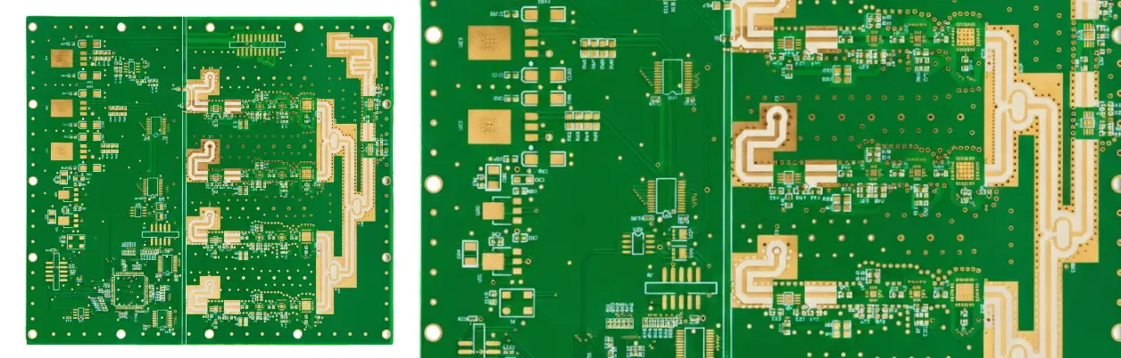
High-Frequency PCB Stackup and Lamination Manufacturability
RF laminate processing can differ from conventional FR-4 in drilling, desmear or surface activation, bonding, resin-flow behavior and dimensional movement. Hybrid constructions add another interaction between materials. The fabrication review therefore checks annular-ring margin, copper balance, registration demand, bonding layers and mechanical tolerances as one system.
Transmission-line geometry is reviewed against the proposed pressed thickness and copper construction. When a design uses microstrip, stripline or grounded coplanar waveguide, the quotation can identify the stackup assumptions that must stay controlled through prototype and repeat production.
RF PCB Capability Envelope: Layer Count, Geometry and Testing
HilPCB can review RF builds across up to 60+ layers, 2/2 mil (50 μm) trace/space, ±5% impedance coupons, 1–67 GHz application bands and VNA/S-parameter options above 40 GHz when the material system, geometry, fixture and acceptance method support the requirement. These limits must be checked against the actual released design rather than combined as a default build.
For a HilPCB order, the released stackup and fabrication files determine the applicable envelope: pressed dielectric thickness, finished copper, trace/space, drill and via structure, panel constraints, material availability and test method. Ask the quotation to state the confirmed layer count, finished thickness, minimum geometry, hole window, impedance tolerance, coupon/TDR or VNA scope, inspection records and lead time. This gives procurement a comparable quote and gives the designer a measurable release boundary.
- Buyer check: separate material, special-process, test and report costs instead of comparing a headline layer count.
- Designer check: provide the stackup, reference planes, impedance table, drill map and RF acceptance band before feasibility is judged.
- Change control: require written review for material substitutions, geometry changes or a different measurement fixture.
RF PCB Controlled Impedance, Via Transitions and Copper Roughness
At RF and microwave frequencies, insertion loss and phase behavior are influenced by dielectric loss, copper roughness, etch geometry, surface finish and discontinuities. We review the design inputs that fabrication can control and separate them from system-level performance that depends on connectors, launches, fixtures and the assembled circuit.
Back-drilling or blind-via structures may reduce via-stub effects, but their suitability depends on the layer transition, finished thickness, drill geometry and registration allowance. Impedance coupons and TDR acceptance limits should be defined in the purchase data rather than assumed from a general web-page capability.
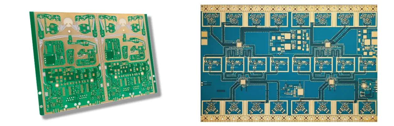
High-Frequency PCB Testing and Documentation Deliverables
Standard fabrication inspection does not replace an RF validation plan. Depending on the order, deliverables may include electrical test, impedance coupon results, TDR traces, microsections, dimensional records, material certificates or lot traceability. VNA or application-specific measurements require agreed fixtures, calibration method, frequency range, test vehicle and pass/fail limits.
HilPCB maintains quality-system and certification records for customer review. Project-specific IPC class, automotive, aerospace or military requirements must be identified in the RFQ and confirmed on the quotation before they become order acceptance criteria. For test-method selection, read our high-frequency PCB testing guide.
RF, Microwave and mmWave PCB Applications
High-frequency PCB manufacturing supports antenna and RF front-end boards, filters and couplers, wireless infrastructure, automotive radar, satellite communications, instrumentation, test hardware and mixed RF/digital systems. Each application places different weight on loss, phase consistency, thermal behavior, repeatability, material availability and documentation.
Share the operating band and the design acceptance criteria with the RFQ. We can then review whether the proposed material, transmission-line structure, via strategy, surface finish and test plan form a manufacturable package.
High-Frequency PCB Prototype-to-Production Handoff
The first build should establish a controlled manufacturing baseline, not just prove that a board can be fabricated once. Approved material, stackup revision, impedance features, coupons, deviations and inspection scope are recorded so repeat orders can reference the same technical package.
If later production requires a material substitution, geometry change or different test scope, the effect should be reviewed before release. This change-control approach helps engineering, purchasing and manufacturing distinguish an approved alternative from an unplanned process change.
- Prototype review: close stackup, material and data questions
- Order definition: document acceptance and report requirements
- Repeat builds: reference the approved revision and agreed controls
Frequently Asked Questions
What files do you need to quote a high-frequency PCB?
Can you build Rogers, PTFE and hybrid RF / FR-4 PCBs?
Can you guarantee my target impedance from a datasheet stackup?
Do all high-frequency PCB orders include VNA testing?
How do you choose between back-drilling and blind vias?
What is the lead time for an RF or microwave PCB?
Experience Advanced PCB Manufacturing Excellence
From simple prototypes to complex production runs, our world-class factory delivers superior quality, fast turnaround and competitive pricing. Join thousands of satisfied customers who trust us with their PCB manufacturing needs.