
Rogers PCB Manufacturer | RF & Microwave PCB | RO4350B, RO4003C & RT/duroid 5880
Rogers PCB and pcb rogers builds from an agile manufacturer. HilPCB delivers fast-turn Rogers PCB fabrication and volume manufacturing of pcb rogers boards. We process RO4350B, RO4003C, RO3003, and RT/duroid laminates with hybrid Rogers + FR-4 stackups, ±5% impedance control, and 24–48h fast dispatch for standard Rogers circuit board builds.
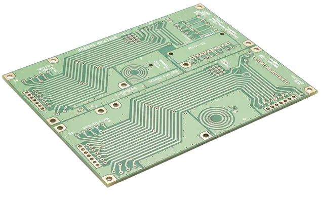
Why Choose Rogers for High-Frequency Performance?
Low loss, stable Dk, predictable phase—engineered for RF/microwaveAs a specialized high frequency PCB manufacturer, HilPCB bridges the gap between electromagnetic simulation and volume production. Engineering a reliable Rogers circuit board requires strictly controlling dielectric constant tolerances and copper roughness losses. Compared with standard FR-4 PCB, Rogers laminates deliver ultra-low dielectric loss (Df typically 0.0009–0.004 at 10 GHz) and stable dielectric constant (Dk variation within ±2%), preserving insertion/return loss and phase accuracy across RF and microwave bands. For frequencies between 5–40+ GHz, Rogers materials such as RO4350B, RO4835, and RT/duroid series maintain predictable line geometry and impedance consistency, critical for radar, 5G front-ends, and satellite communication systems.
We maintain standard processing for common laminate thicknesses (including RO4350B at 10, 20, 30, and 60 mil, and RO4003C at 8, 12, 20, and 32 mil), enabling 24–48h quickturn prototype fabrication. Our process flow—plasma activation of PTFE composites, surface roughness control with low-profile copper (Ra ≤1.5 μm), and precision lamination pressure profiling—supports hybrid stackups that place Rogers where RF energy travels, while internal planes use multilayer FR-4 cores to reduce material cost by 30–50%. See our Rogers PCB guide and stackup design notes for detailed layer planning methods.
Critical Risk: Poor PTFE adhesion, misaligned bond films, or excessive lamination temperature gradients can cause voiding, layer shift, or Dk drift during fabrication. These effects increase reflection loss and phase error, particularly above 10 GHz.
Our Solution: We implement lamination process control with plasma pre-cleaning, differential pressure lamination, and in-situ temperature sensors to ensure bondline uniformity. Signal integrity design simulations and TDR-based impedance validation correlate simulation with measured data for production tuning. Hybrid builds with selective PTFE use balance RF performance, cost, and manufacturability.
For extreme RF/mmWave systems—radar, 5G front-ends, and aerospace communication—Rogers boards pair seamlessly with our high-frequency PCB and ceramic PCB lines to extend thermal and electrical stability across 24–110 GHz ranges.
- RO4000®, RO3000® and RT/duroid® series support
- Insertion loss targets below ~0.5 dB/in at 10 GHz (design dependent)
- Backdrill to <10 mil to remove stubs
- Impedance coupons correlated to field solver results
- Hybrid cost optimization with RF-critical layers in Rogers
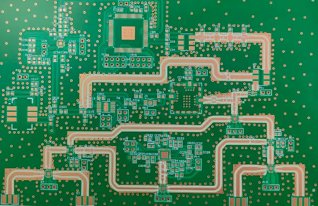
🚀 Quick Quote Request
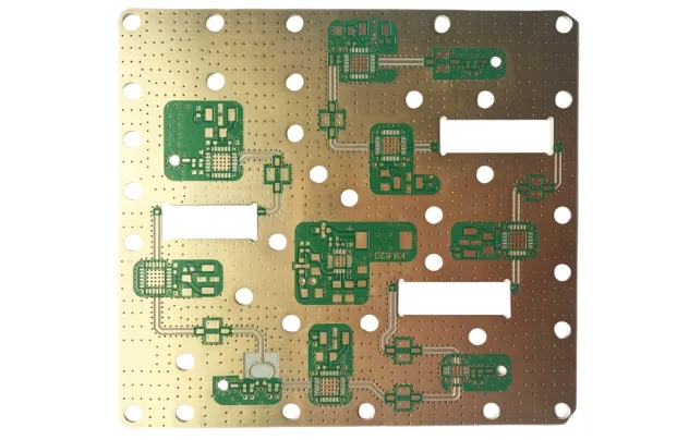
📋 Get Full Capabilities
Specialized RF/Microwave Manufacturing Controls
PTFE handling, low-profile copper, staged laminationPTFE and ceramic-filled laminates require tailored controls: plasma etch for hole-wall activation (adhesion typically >1.0 N/mm), staged pressure/temperature profiles (e.g., 175–185 °C), and controlled-depth drilling for launch transitions. UV-laser microvias (75–100 μm) and backdrill remove resonant stubs for 25+ Gbps channels.
Quality verification includes TDR for impedance (±5%) and sample-based VNA S-parameters (S11/S21) commonly up to 40 GHz. Microsections confirm ≥20 μm barrel copper; ionic contamination is held ≤1.56 μg/cm². See high-frequency PCB testing and impedance testing.
- Low-profile/VLP copper to cut conductor loss by ~10–25%
- Backdrill & launch optimization for low reflection
- TDR-verified coupons on every panel (when specified)
- VNA S-parameters for RF prototypes
- Documentation aligned with IPC-6018 workflows
Rogers PCB Technical Specifications
Rogers material, geometry and test options for RF, microwave and mmWave designs
| Decision Area | Standard Route | Advanced Review | Confirmation Basis |
|---|---|---|---|
Layer Count | 1–28 layers | Up to 50 layers; hybrid stackups | IPC-6018 |
Base Materials | RO4003C™, RO4350B™, RT/duroid® 5880 | RO3003™, RO3010™, Taconic, Isola; hybrids with FR-4 | IPC-4103 |
Dielectric Constant (Dk) | ≈2.2–10.2 | Tight-tolerance Dk materials | Material datasheet |
Loss Tangent (Df) | <0.004 @ 10 GHz | Ultra-low loss <0.002 | Material datasheet |
Board Thickness | 0.20–3.20 mm | 0.10–6.00 mm, ±5% tolerance | IPC-A-600 |
Copper Weight | 0.5–2 oz | Up to 4 oz; VLP copper options | IPC-4562 |
Min Trace/Space | 75/75 μm (3/3 mil) | 50/50 μm (2/2 mil) | IPC-2221 |
Min Hole Size | 0.20 mm | 0.10 mm + backdrill | IPC-2222 |
Impedance Control | ±10% | ±5% or tighter | IPC-2141 |
Surface Finish | ENIG, Immersion Silver, OSP | ENEPIG, Soft/Hard Gold | IPC-4552/4553 |
Quality Testing | 100% E-test, TDR impedance | VNA S-parameters, ionic contamination | IPC-9252 |
Certifications | ISO 9001, UL, IPC Class 2 | AS9100, MIL-PRF-31032, IPC Class 3 | Industry standards |
Lead Time | 7–15 days | 24–48h dispatch for standard core thicknesses | Production schedule |
Need capabilities beyond this product? Explore our full manufacturing capabilities
Ready to start your PCB project?
Whether you need simple prototypes or complex production runs, our advanced manufacturing capabilities ensure excellent quality and reliability. Get your quote within 30 minutes.
Signal Integrity by Design
Use field solvers with the laminate supplier's recommended copper-roughness model and validate the released geometry with coupon TDR when specified. Keep return-via placement and launch geometry consistent with the modeled transition. For high-rate links, pair with high-speed PCB review and plan backdrill to residual stubs <10 mil where the analysis requires it. See impedance testing and advanced RF design.
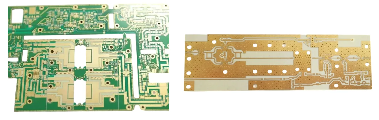
Custom Rogers PCB for RF and Microwave: Transitions, Grounding and Fabrication Control
A custom Rogers PCB usually fails for mechanical rather than electrical reasons: a launch that was never modelled, a ground plane interrupted by a via fence, or copper surface roughness that was ignored in the loss budget. Addressing those three items during design is what makes a Rogers PCB fabrication service predictable.
Transitions and launches. Where a signal leaves the laminate — into a connector, a cable or a different dielectric — the discontinuity dominates the response. Design the launch with the same controlled impedance as the trace and validate it with a calibration coupon on the same panel. For microwave work, define the coupon and the required TDR/VNA outputs in the RFQ so they are part of the agreed deliverables.
Grounding and via strategy. Grounded coplanar waveguide needs a dense, symmetric via fence tied to a continuous reference plane. Asymmetry creates common-mode radiation that shows up as unexpected emissions later. Where the design uses microstrip-to-stripline transitions, the layer stack must be defined before the routing is drawn.
Fabrication control on low-loss materials. PTFE laminates are soft and prone to dimensional movement, so panel design, drill parameters and surface preparation must be tuned to the material. Copper foil type affects conductor loss at higher frequencies; standard foil and low-profile foil are not interchangeable in a tight loss budget. Plating and surface finish choices also interact with the laminate — discuss these manufacturing controls with our engineers before releasing artwork.
When the RF front end sits beside dense digital control, evaluate HDI or a hybrid stack so the controlled-impedance portion stays small. For frequency-sensitive mechanical constraints, compare PTFE laminate options.
If the loss budget or the launch geometry is still open, put the stackup and the frequency band into the RF stackup review before artwork release; we will confirm the laminate, copper foil type and thickness tolerance that the design actually needs.
Choosing the Right Rogers Material
As an agile RF PCB manufacturer, HilPCB reviews grade properties against operating frequency, loss budget, and assembly methods:
RO4350B™ (Dk ~3.48; Df ~0.0037 at 10 GHz) is our most frequently fabricated ceramic-filled hydrocarbon laminate. It combines low dielectric loss with standard FR-4 processing and UL 94V-0 flame retardance, making it ideal for 5G power amplifiers, RF front-ends, and commercial wireless infrastructure.
RO4003C™ (Dk ~3.38; Df ~0.0027 at 10 GHz) provides ~27% lower dielectric loss and higher thermal conductivity than RO4350B for tighter loss margins.
RT/duroid® 5880 (Dk ~2.20; Df ~0.0009) supports very-low-loss microwave and mmWave designs up to Ku, Ka, and W-bands.
RO3003™/RO3010™ provide PTFE-ceramic stability benchmarked for 77 GHz automotive radar. A hybrid stackup can reserve Rogers for RF microstrip layers and use FR-4 for power or digital routing, reducing raw board cost by 30–50%. See our guide on microwave loss budgeting.
Rogers PCB Material Selection: Price, Dk/Df Targets and FR-4 Hybrid Stackups
Specifying a Rogers PCB is a material decision before it is a fabrication decision. The family spans laminates with very different dielectric constants, loss tangents and processing behaviour, and the cost spread between them is large. Choosing correctly starts from the electrical requirement, then gets reconciled against price and manufacturability.
Which Rogers PCB material for which job. PTFE-based laminates such as RT/duroid 5880 deliver the lowest loss for millimetre-wave and high-frequency work, but they are soft, dimensionally active and comparatively expensive. Hydrocarbon/ceramic materials like RO4350B and RO4003C give stable Dk with much easier processing, which makes them the usual choice where a high-frequency Rogers PCB must also be a volume part. When the requirement is broadband performance across a wide temperature range, the material properties must be evaluated at your operating conditions rather than at 10 GHz alone.
Rogers FR-4 hybrid stackups. A Rogers FR-4 hybrid PCB uses low-loss material only where the RF path runs and standard FR-4 elsewhere, which controls cost without compromising the critical nets. A mixed FR-4 + Rogers stackup requires careful attention to lamination compatibility, coefficient-of-thermal-expansion mismatch and drill registration across dissimilar materials. A multilayer Rogers or hybrid build must also define how impedance is referenced when a signal transitions between the two dielectrics.
Country of manufacture and sourcing. Choosing a Rogers PCB supplier, in China or locally, comes down to lead time and landed cost as much as the laminate brand. HILPCB verifies the Rogers grade and certificate of conformance for each build and can advise on alternatives when a specific grade is constrained — see the high-frequency PCB page for laminate and stackup options.
Thermal and RF requirements converge on power amplifiers, where the laminate sets the electrical behaviour but the heat still has to leave the board. For those designs the mechanical and thermal half of the problem is handled by metal core and aluminum PCB constructions, often as a hybrid with the RF laminate.
Rogers PCB Engineering Examples for RF Release Planning
These common engineering scenarios show how HilPCB can review Rogers grade, bond material, copper, launches and RF evidence against one released stackup. The quotation defines the applicable material route and measurement scope.
77 GHz automotive radar antenna boards. Design Dk/Df method, copper profile, line geometry, antenna region, via transitions and radome or assembly constraints must remain aligned. Use the mmWave antenna array PCB guide to prepare material, launch, backdrill and VNA requirements.
5G radio and beam-forming modules. A hybrid RO4350B and FR-4 construction can separate RF, power and digital functions, but bondply, registration, phase tracking and thermal paths must be reviewed together. The RO4350B PCB example organizes the stackup and coupon decisions.
RF prototypes and test instrumentation. Material substitutions, connector launches, calibration planes, de-embedding and repeatable coupon placement determine whether measured S-parameters support the design decision. See the Rogers PCB prototyping example when defining the release and test package.
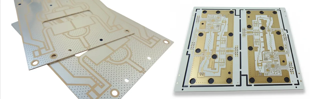
Advanced RF Quality Assurance
Beyond AOI/E-test, sample-based VNA characterizes S-parameters (S11/S21) up to ~40 GHz; TDR verifies characteristic impedance within ±5%. Microsections confirm via plating thickness (≥20 μm) and registration (±50 μm typical). Ionic contamination targets ≤1.56 μg/cm². Learn more in our high-frequency PCB testing methods.
Engineering Assurance & Certifications
Experience: RF builds can use coupon-to-solver correlation and hybrid stackup review when the electrical targets and coupon design are supplied.
Expertise: the process review covers material-specific surface preparation, low-profile copper, lamination, controlled-depth drilling and backdrill.
Authoritativeness: workflows can be aligned with IPC-6018 and quotation-defined AS9100 program documentation.
Trustworthiness: specify the required material lots, traveler, coupon, VNA or TDR data and retention period in the RFQ; HilPCB confirms which records are included.
Rogers PCB RFQ Requirements
Send the latest Gerber or ODB++ package, NC drill data, fabrication drawing and proposed stackup. Name the Rogers grade and thickness, approved substitutes, bondply or prepreg, copper profile and weight, surface finish, quantities and delivery target.
Include Dk/Df method and frequency, impedance table, loss or phase targets, backdrill and launch details, coupon design and required TDR/VNA outputs. Up to 50 layers, 50/50 µm geometry, hybrid construction and mmWave testing are not automatically combinable; engineering confirms the applicable route after material and file review.
Rogers PCB Testing and RF Deliverables
Material identity can be supported by the specified Rogers grade and CoC; plated-hole quality by microsection; controlled impedance by coupon TDR; and RF response by sample VNA S-parameters over an agreed range. Ionic cleanliness or thermal records can be included when required.
Define reference planes, de-embedding, fixture, sample plan, limits, data format and report retention in the RFQ. HilPCB identifies included and optional evidence in the quotation.
Frequently Asked Questions
When should I choose Rogers instead of FR-4?
What are the benefits of a hybrid Rogers + FR-4 stackup?
Do you provide S-parameter measurements?
How do you control via stub effects at high frequency?
Which finishes are recommended for RF pads?
What is a Rogers FR-4 hybrid PCB?
Experience Advanced PCB Manufacturing Excellence
From simple prototypes to complex production runs, our world-class factory delivers superior quality, fast turnaround and competitive pricing. Join thousands of satisfied customers who trust us with their PCB manufacturing needs.