
What to Prioritize First for 3oz Heavy Copper PCB Volume Production
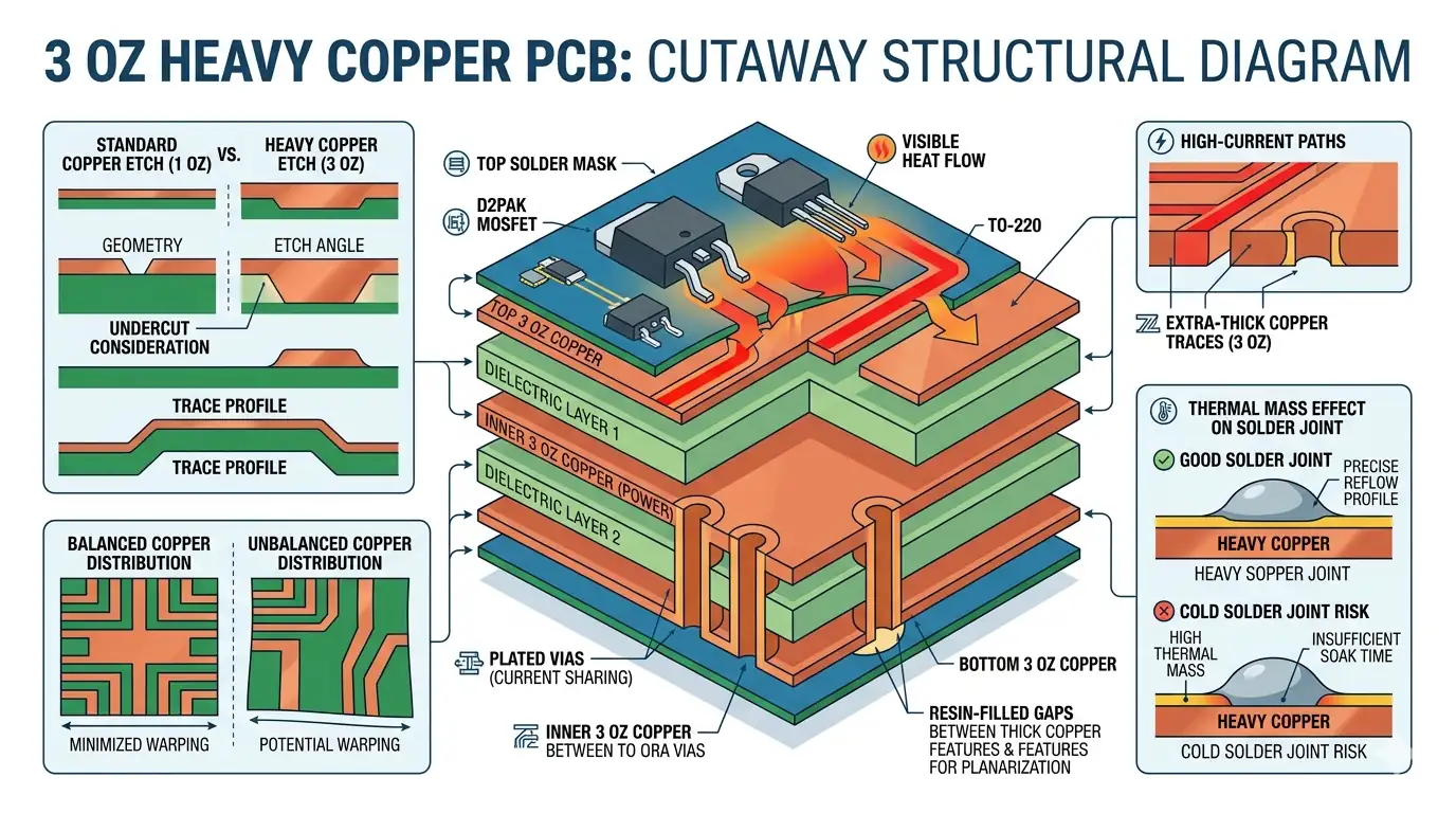
When transitioning a 3oz heavy copper PCB into volume production, the primary question is not simply "can the factory build 3oz," but whether the high-current path, etching compensation, resin fill during lamination, structural symmetry, and assembly thermal mass can all converge successfully within a single process window. As copper thickness increases, trace cross-sections, resin flow kinetics, copper balancing, and soldering heat absorption become exponentially more sensitive. Consequently, successfully yielding a prototype board does not guarantee that mass production will sustain the same reliability and consistency.
Validation Directory
- Why High-Current Paths Are More Than Just Main Trace Width
- Why 3oz Heavy Copper Amplifies Etching Compensation Challenges
- How Lamination Fill and Structural Symmetry Determine Board Stability
- Why Heavy Copper Is Not a Universal Thermal Management Solution
- The Importance of Evaluating Assembly Thermal Mass Before SMT
- Frequently Asked Questions (FAQ)
- Next Steps: Initiating Heavy Copper DFM and Assembly Reviews
3oz Heavy Copper PCB: DFM Review Summary
| Risk Dimension | Public Benchmark / Standard | Project-Level DFM Focus | Engineering Reminder |
|---|---|---|---|
| Thickness & Profile | The industry references 3 oz/ft² as ~`105 µm` nominal thickness. |
Actual trace cross-sections, lateral etch compensation, and final current-carrying capacity must be verified against factory capabilities. | Nominal thickness cannot substitute for real cross-sectional evaluation. |
| Lamination Fill | Heavy copper layouts rely critically on prepreg resin flow and localized balancing. | Disproportionate thick-copper routing, vast voids, and deep intra-layer trenches amplify resin starvation and void risks. | Evaluate resin fill capability alongside copper balancing. |
| Warpage & Symmetry | IPC-6012 outlines baseline Bow & Twist tolerances. | Heavy copper projects require holistically judging copper distribution, layer symmetry, and lamination stress. | Structural symmetry dictates post-press flatness. |
| Assembly Thermal Mass | Thick copper drastically alters heat absorption dynamics during soldering. | Pad thermal reliefs, preheating curves, component thermal loads, and fixture supports must be confirmed collectively. | You must recalculate thermal mass windows for heavy copper SMT. |
Why High-Current Paths Are More Than Just Main Trace Width
When analyzing high-current paths, scrutinizing the width of the main trace polygon is insufficient because current flow and thermal runaway are rarely limited by the widest sections. The true constraining bottlenecks emerge at connector pins, component neck-downs, layer-transition via arrays, and localized narrowing geometries. If these zones are not systematically mapped alongside the main trace, widening the bulk copper path merely forces heat and voltage drops into the most fragile junctions. Based on the IPC-2152 current carrying capacity framework, the core priority is evaluating localized cross-sectional bottlenecks and thermal environments, instead of assuming nominal trace widths denote safety.
For high-current copper balancing and stackup design, practical DFM pre-checks proactively investigate:
- Are there aggressive neck-downs before the main circuit enters MOSFETs, shunts, connectors, or fuse elements?
- When high currents transfer between layers, are the via count, hole diameter, plating thickness, and return proximity adequate?
- Do main power rails share forced, narrow pathways bordering sensitive control signal routing?
- With the transition to 3oz thickness, have voltage drop, thermal rise, and localized dissipation been computed using the real etched cross-section rather than the ideal geometry?
Consequently, the optimal approach to a 3oz heavy copper design is not "uniformly thickening every layer," but systematically isolating the actual current bottlenecks, specifying precisely which features require widening, dual-layer sharing, or targeted localized heavy copper reinforcement.
Why 3oz Heavy Copper Amplifies Etching Compensation Challenges
Heavy copper magnifies etching compensations because thicker metal necessitates prolonged chemical etching, dramatically escalating the lateral undercut (etch factor) and distorting the targeted rectangular trace profile into a trapezoid. If a designer imports standard thin-copper fine-line capabilities into a 3oz layout, the board will suffer from severe cross-sectional shrinkage, residual shorts between narrow gaps, or inadequate dielectric clearances during mass production.
In public technical literature, a common anchor for heavy copper assumes 3 oz/ft² yields roughly a 105 µm nominal thickness. However, citing this static value does not substitute for DFM judgment, because the operational viability depends on:
- Whether the traces reside on external or internal layers.
- If expansive copper pours intersect closely with dense, fine-pitch control signals.
- The fabricator’s precise CAM compensation scaling, localized etching capacity, and micro-sectioning verification methods.
- The project's required dielectric margins to ensure long-term, high-voltage reliability.
For Heavy Copper PCB projects, the robust methodology expects designers to conservatively evaluate trace widths and isolation distances, utilizing factory-verified CAM etching compensation adjustments. Referencing universal frameworks like IPC-2221B provides baseline principles but will not automatically generate the tight manufacturing windows unique to heavy copper profiles for your specific manufacturer.
Process Derisking (Do vs Don't)
❌ Don't: Blindly copy-paste fine-line spacing rules cleared for standard 1oz logic boards onto a 3oz heavy-current layout. ✅ Do: Initiate an early DFM review to align target thickness, routing distribution, CAM compensation factors, and allowable cross-section tolerances before locking the layout design rule check (DRC).
How Lamination Fill and Structural Symmetry Determine Board Stability
Resin fill behavior and structural symmetry dictate heavy copper board stability because 3oz layers amplify localized topographical height discrepancies, altering resin flow paths and imbalancing lamination stress. If disproportionate thick copper areas, vast voided regions, and asymmetrical layer definitions are pressed blindly, initial pilot runs will expose severe subsurface voids, resin starvation, acute bowing, or layer-delamination under thermal stress.
Within Multilayer Heavy Copper Board architectures, engineering focus pivots toward:
- Whether deep thick-copper trenches obstruct the underlying prepreg from achieving a stable volumetric fill.
- Identifying if immense copper-free zones situated adjacently to dense copper planes inflict uneven lamination pressures.
- Ensuring the layer stackup possesses robust symmetry to neutralize post-lamination bow and twist from multiplying.
- Implementing deliberate copper thieving (balancing squares), dummy planes, or localized structural aids to harmonize resin flow.
When a PCB houses large ground planes alongside open routing gaps, "it can be pressed" is a poor benchmark for success. The rigorous target is: under volume production tolerances, aligning the stackup, copper balancing, and resin system to support a stable geometric profile. Relying on IPC-6012 Delivery Frameworks, heavy copper products must fundamentally deliver reliable flatness, structural integrity, and repeatable batch consistency.
Why Heavy Copper Is Not a Universal Thermal Management Solution
Thermal design cannot simply default to thickening copper as a universal cure because heavier copper predominantly enhances in-plane thermal spreading (X-Y axis), but it does not automatically resolve component junction temperatures, vertical z-axis thermal paths, or localized cross-coupling. Without integrating thermal vias, specific interface materials, thoughtful component placement, and heatsink mechanicals, relying on thick copper alone ignores the comprehensive systemic thermal challenge.
For traceable thermal-management control in power-cooling systems, critical audits entail verifying:
- Whether heat sources actively dissipate vertical load through designated via arrays, embedded copper coins, or chassis structures.
- Checking for localized routing restrictions or narrowed paths near high-heat devices severely throttling lateral heat flow.
- Evaluating whether upgrading to 3oz inadvertently aggravates localized assembly complications and mechanical shear stresses at the component pad.
- Ensuring the baseline material system correlates with sustained high-temperature thermal cycling, lamination structure, and final ambient conditions.
Thus, addressing thermal resilience on 3oz heavy copper boards requires framing the discussion correctly: thick copper is an excellent mechanism for current carrying and planar heat distribution, but it must be co-engineered with component placement, direct conductive paths, and material properties—"3oz" is not synonymous with "heat solved."
The Importance of Evaluating Assembly Thermal Mass Before SMT
SMT assembly teams must evaluate heavy copper board thermal mass in advance because extensive thick-copper regions drastically alter the heat absorption profile (thermal demand) of the pads and the board itself. If thermal reliefs (pad connections), board thermal mass, and reflow oven profiling are still processed with standard-board logic, the PCBA will suffer from poor wetting, cold solder joints, inconsistent wetting angles, and a dangerously restrictive process window.
For PCB Assembly DFM, the 3oz front-end checks commonly include:
- Scrutinizing whether surface pads directly flooding into large copper planes mandate engineered Thermal Reliefs to prevent localized heat sinking.
- Determining if massive terminals, high-power FETs, and bulky high-thermal-mass components demand specialized profiling instructions.
- Realizing that pre-soak times, ramp-up speeds, and peak reflow zones explicitly require recalibration for the board's escalated thermal density.
- Confirming that SMT carriers, fixtures, and localized board supports won't generate shadow zones affecting uniform reflow.
Consequently, the professional manufacturing paradigm for heavy copper avoids "adjusting the oven profile to save the board" during pilot runs. Instead, pad connectivity, the BOM's thermal limits, and assembly-reflow dictates must be integrated systematically before the layout is released.
Frequently Asked Questions (FAQ)
Q: Does specifying a 3oz heavy copper PCB guarantee adequate current carrying capability?
A: Not implicitly. Increasing copper thickness drastically supports higher current limits, but true bottlenecks frequently dictate limits—namely neck-downs, via transition arrays, connector geometries, and constrained thermal environments. Heavy copper is an asset but does not replace exhaustive current-thermal assessments.
Q: Can a 3oz design maintain the identical fine-line trace/space parameters of a standard 1oz logic board?
A: It is highly discouraged. Increased copper obligates lateral etching allowances and cross-sectional loss estimations to be addressed beforehand. While prototypes may occasionally clear narrow spacing, it yields disastrously low success rates and degraded isolation margins in high-volume production.
Q: Why do heavy copper multilayer boards suffer elevated risks regarding resin fill voids and warpage?
A: A 3oz layer drastically amplifies localized Z-axis topographical height gaps, worsening uneven lamination pressure. If heavy-copper zones, resin-starved voids, and cross-layer geometries remain asymmetrical, prepreg flow turns erratic, guaranteeing severe mechanical warpage.
Q: Doesn't a thicker copper layer mean much more reliable solder joints during SMT?
A: It actually presents a severe assembly challenge. Thick copper aggressively conducts heat away from the pad during SMT. If pads lack thermal reliefs, or if preheat curves are insufficient, heavy copper induces cold-soldering, inadequate wetting, and drastically narrows the viable reflow window.
Q: What must be decisively verified prior to releasing a heavy copper mass production run?
A: Always verify main-circuit bottlenecks, specific etching compensation bounds, lamination resin-fill systems, symmetrical copper balancing, and specialized high-mass component reflow profiles. Synchronizing fabrication limits and assembly boundaries early radically suppresses scrap rates during initial builds.
Next Steps: Initiating Heavy Copper DFM and Assembly Reviews
When your design utilizes 3oz heavy copper, high-current power stages, motor control drives, or robust server backplanes, ensuring reliability demands moving past generic "Can you manufacture 3oz?" inquiries. A comprehensive pre-manufacturing review requires synthesizing:
- Formal ODB++ / Gerber data paired with full stackup definitions.
- Documentation illustrating main current networks, key high-power MOSFETs, and layer transitions.
- A highlight of thick-copper distributions, sprawling copper planes, and assembly-sensitive surface pads.
- Intended component packages, assembly methodologies, and pilot-level validation goals.
Correlating these elements with the Heavy Copper Product Capabilities, Multilayer Fabrication Matrices, and High-Tg Material Selection guides correctly identifies standard process limits versus stringent DFM parameters strictly required for your specific high-mass layout.
If you must qualify a 3oz heavy copper structural check, mandate etching compensations, or pre-assess thermal reflow risks before committing to first-article fabrication, submit your routing, stackup, and crucial current paths directly to our Engineering Team for a synchronized fabrication and assembly evaluation.
Advanced DFM Documentation:
- Heavy Copper PCB Structure and Production Overview
- Multilayer PCB Stackup & Structural Symmetry Guide
- High-Tg PCB Material Selection for Heavy Loads
*Author: HILPCB High-Speed Interconnect Engineering Team* *Reviewed by: HILPCB SI/DFM Engineering Team* *Last Updated: 2026-04-02*