
High-Tg PCB Manufacturer | Tg 170–200 °C Multilayer Boards
High-Tg PCB manufacturing for lead-free reflow, automotive, industrial and power-electronics programs. HilPCB reviews Tg, Td, Z-axis CTE, copper, via structure, thermal profile and required test records together before confirming the material and build route.
Capabilities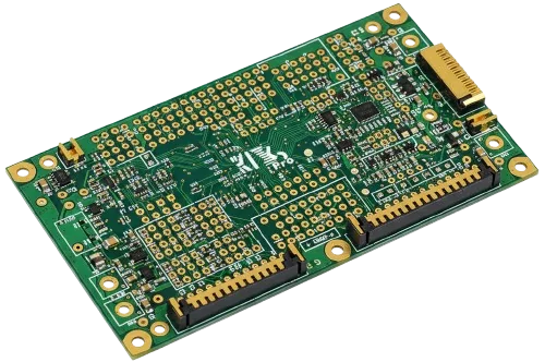
High-Tg PCB Material Selection: Tg, Td, CTE and CAF Risk
Tg is one input; the released laminate and thermal profile define the usable constructionA high-Tg PCB uses a resin system with a higher glass-transition temperature than standard FR-4. It is commonly reviewed for repeated lead-free reflow, dense multilayers, heavy copper, automotive electronics, industrial power and other builds where Z-axis expansion or resin stability can reduce via and lamination margin.
Tg does not describe thermal reliability by itself. HilPCB reviews decomposition temperature (Td), Z-axis expansion, time-to-delamination data, moisture behavior, CAF requirement, copper distribution, via aspect ratio and the actual assembly profile. Supplier datasheet values remain material-selection references; they do not define finished-board performance.
Specify the required manufacturer and grade, approved substitutes and applicable test method when those details affect qualification. If high temperature is continuous rather than an assembly excursion, engineering may recommend polyimide, ceramic PCB or another construction instead of treating a higher Tg number as the complete solution.
- Tg 170–180 °C standard high-Tg route; ≥200 °C materials by review
- Td and Z-axis expansion checked with the supplier datasheet
- Assembly reflow count, peak and dwell included in material review
- CAF, CTI, flammability and halogen requirements confirmed when applicable
- Copper balance, resin fill and via structure reviewed with the stackup
- Approved laminate and substitution rule recorded with the order
🚀 Quick Quote Request
📋 Get Full Capabilities
High-Tg Multilayer Lamination, Drilling and Via Review
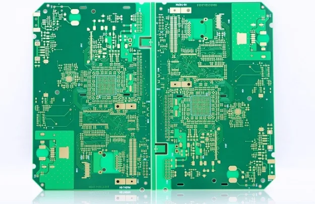
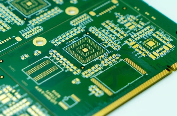
Material, copper, geometry, vias and schedule are approved as one constructionHigh-Tg prepregs can have different resin-flow, cure and moisture-handling requirements from standard FR-4. The manufacturing review therefore checks glass style, resin content, copper distribution, fill around heavy features, lamination sequence, finished thickness, registration and drill aspect ratio before the press cycle is released.
The capability envelope includes 40+ layers, 0.5–6 oz copper, 3/3 mil advanced geometry and 0.15 mm mechanical holes, but these limits are not automatically combinable. A dense 40-layer build, heavy copper, fine geometry and short lead time may require different material, panel or via choices. HilPCB returns the approved stackup and DFM questions before order release.
For high-current regions, coordinate the high-Tg material with heavy-copper PCB review. For loss-sensitive links, compare the selected high-Tg FR-4 with low-loss or high-frequency materials instead of assuming Tg predicts Dk or Df.
- Tailored lamination ramps for each resin system
- Pre-bake and MSL-grade storage to control moisture
- Registration and drill tolerances confirmed for the released stackup
- Microsection or thermal records available when included in the quality plan
- Expedite eligibility confirmed after material and file review
High-Tg PCB Manufacturing Capabilities
Use listed values for design screening and advanced limits only after combined review
| Decision Area | Standard Route | Advanced Review | Confirmation Basis |
|---|---|---|---|
Layer Count | 2–28 layers | 40+ layers | Released stackup and lamination review |
Base Materials | High-Tg FR-4 such as S1000-2M or IT-180A; Tg ≥170 °C | Polyimide, Megtron 6, RO4350B | Approved material list, grade and supplier datasheet |
Glass Transition Temp (Tg) | 170–180 °C | 200 °C class and specialty materials by review | Supplier datasheet and stated Tg test method |
Decomposition Temp (Td) | ≥340 °C material screen | >360 °C material options | Supplier datasheet and stated Td test method |
Board Thickness | 0.6–3.2 mm design screen | 0.4–6.0 mm by stackup and handling review | Fabrication drawing and pressed stackup |
Copper Weight | 1–3 oz | 0.5–6 oz including heavy-copper review | Copper distribution, geometry and resin-fill review |
Min Trace/Space | 100/100 μm (4/4 mil) | 75/75 μm (3/3 mil) on eligible constructions | Finished copper, etch and panel review |
Min Hole Size (Mechanical) | 0.20 mm | 0.15 mm by aspect-ratio review | Drill file, finished thickness and plating requirement |
Max Panel Size | 571.5 × 609.6 mm | 571.5 × 1200 mm | Panel drawing, copper balance and equipment route |
Surface Finish | Lead-Free HASL, ENIG, OSP | Immersion Silver, ENEPIG, Hard Gold | Assembly, storage, contact and bonding requirements |
Quality Testing | Visual/AOI and electrical test plan | Thermal stress/cycle, TMA/DSC, IST, TDR or microsection when quoted | Purchase specification and quality plan |
Certifications | ISO 9001, UL, RoHS/REACH | IATF 16949, AS9100, ISO 13485 | Applicable certified site, quotation and quality agreement |
Lead Time | Confirmed after material and fabrication-file review | Expedite route for eligible constructions | Approved files, material availability and production schedule |
Order Deliverables | Approved stackup, material and build requirements recorded with the order | Material CoC, thermal record, IST/TDR data or microsection when quoted | RFQ deliverable list and purchase order |
Ready to start your PCB project?
Whether you need simple prototypes or complex production runs, our advanced manufacturing capabilities ensure excellent quality and reliability. Get your quote within 30 minutes.
High-Tg PCB Via Reliability and Reflow Review
Via reliability depends on the laminate's Z-axis expansion, finished board thickness, hole diameter, plating requirement, copper wrap, via fill and the number and severity of assembly or field thermal cycles. HilPCB reviews these inputs together and identifies aspect-ratio, resin-fill or material changes before release.
When the program requires objective evidence, define the acceptance method in the RFQ. Options can include microsection, solder-float or thermal-stress records, IST, thermal cycling and resistance-change criteria. The test condition, sample plan, limits and report format must be agreed; selecting a high-Tg material does not by itself define cycle life.
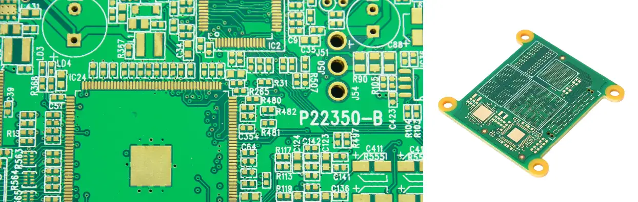
Standard FR4 vs High-Tg FR4, Polyimide and Low-Loss Materials
- Standard FR4: appropriate when the normal assembly profile and operating environment leave adequate thermal margin.
- High-Tg FR4: review for repeated lead-free reflow, dense multilayers, higher copper mass, reduced Z-axis expansion or demanding humidity/CAF requirements.
- Polyimide: consider for sustained high-temperature or severe cycling programs where the complete material system, not Tg alone, justifies the added process and cost.
- Low-loss high-Tg material: use when both thermal stability and channel loss matter; confirm Dk/Df method, copper profile and stackup with the electrical model.
- Ceramic or metal-backed construction: consider when thermal conductivity or heat spreading is the primary problem, because high Tg does not make FR4 a high-conductivity material.
High-Tg PCB Failure Modes and Acceptance Planning
The review should connect each risk to a control and an acceptance record: resin cure and delamination to material/press data, via fatigue to geometry and microsection or IST, CAF risk to material/spacing/moisture requirements, bow and twist to copper balance and panel handling, and impedance drift to the released stackup and coupon method.
IPC class, test method and customer specification are not interchangeable. State the applicable revision, class, sampling, thermal condition and pass/fail limits in the purchase data. See our IPC Class 3 guidance and thermal-shock testing overview when defining the required evidence.
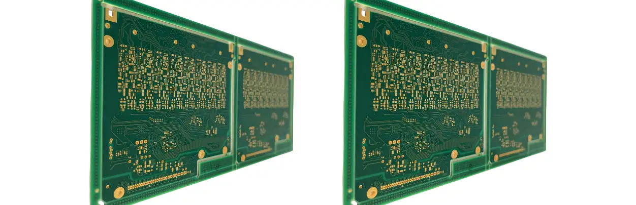
High-Tg PCB Engineering Examples for Thermal-Reliability Review
These common engineering scenarios show how HilPCB can review a high-Tg build around the actual thermal exposure, copper distribution, via structure and acceptance plan. The quotation confirms the released material, construction and evidence.
EV charger and BMS boards. Heavy copper, repeated lead-free reflow and field temperature cycling require Tg, Td, Z-axis CTE, resin fill, via aspect ratio and copper balance to be reviewed together. Use the EV on-board charger PCB example to prepare thermal-profile, high-voltage and inspection inputs.
Industrial drives and power controls. Localized heat, high-voltage spacing and contamination risk can make CTI, CAF, moisture handling and material traceability as important as the Tg value. The CTI material-selection example organizes the insulation and acceptance questions.
Dense communications and compute boards. A design may need both thermal stability and lower channel loss. Stackup, Dk/Df method, copper profile, impedance coupons and reflow exposure should share one release baseline; see the CPO baseboard example for the combined material and signal-integrity review.
High-Tg PCB Certification and Traceability Scope
HilPCB supports ISO 9001, UL, IATF 16949, AS9100 and ISO 13485 program requirements within the applicable certified site and agreed project scope. State the required certificate, IPC class/revision, PPAP or medical record set, material traceability, lot identification and change-notification rules in the RFQ.
Depending on the quotation, the evidence package can include the released stackup, material declaration or CoC, traveler/lot reference, inspection record, electrical-test confirmation, thermal record, microsection or other agreed data. Certification does not imply that every order automatically receives every report.
High-Tg PCB RFQ Requirements for a Comparable Quote
Send the latest Gerber or ODB++ package, NC drill files, fabrication drawing and proposed stackup. Include layer functions, finished thickness, copper weights, minimum geometry, hole and via structures, surface finish, impedance table, quantities and delivery target.
Define the laminate manufacturer/grade or required Tg, Td, Z-axis CTE, CAF/CTI, flammability and halogen conditions. Add the assembly profile: reflow count, peak temperature, dwell and any rework exposure. State the IPC class/revision, inspection, electrical test, thermal test, material certificate, microsection, IST/TDR data and traceability records required for acceptance.
High-Tg PCB Testing and Deliverables
Evidence should answer the project risk rather than follow a universal bundle. Material identity can be supported by the specified grade and CoC; internal interconnect quality by microsection or IST; assembly resistance by an agreed thermal-stress method; and controlled impedance by coupon/TDR data when required.
List the method, sample plan, condition, acceptance limit and output format in the RFQ. HilPCB confirms which records are included, optional or customer-supplied before quotation, so procurement can compare equivalent scopes and engineering can retain a repeatable release baseline.
Frequently Asked Questions
What is the difference between Tg and Td?
When should I choose High-Tg FR-4 versus polyimide?
Does High-Tg improve heat dissipation?
How does Z-axis CTE affect via reliability?
Which finishes are recommended for High-Tg builds?
What files and thermal information are needed for a High-Tg PCB quote?
What High-Tg PCB test reports can be supplied?
Experience Advanced PCB Manufacturing Excellence
From simple prototypes to complex production runs, our world-class factory delivers superior quality, fast turnaround and competitive pricing. Join thousands of satisfied customers who trust us with their PCB manufacturing needs.