
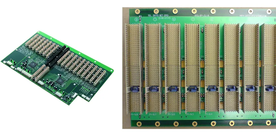
In a tech industry, Artificial Intelligence is undeniably the core engine driving industry transformation. Behind the astonishing capabilities of large language models (LLMs) and complex neural networks lies a massive demand for computational power, which directly drives the continuous evolution of AI server hardware architecture. As a foundational component carrying CPUs, GPUs, memory, and high-speed networks, the complexity of an AI server motherboard far exceeds that of traditional servers. Today, AI server motherboard PCB compliance is no longer just about meeting basic electrical standards; it represents the ultimate test of high-speed signal integrity (SI), extreme power delivery networks (PDN), and advanced thermal management.
For hardware engineers and product managers, ensuring the compliance and reliability of these complex boards is an unprecedented challenge. From navigating the stringent requirements of PCIe 5.0/6.0 to managing the thermal dissipation of kilawatt-class chips, every design decision determines the success or failure of the final product. This article will examine the core technical challenges of AI server motherboards and share proven AI server motherboard PCB guidelines, helping you successfully navigate from design to manufacturing.
The performance leap of AI servers and its impact on PCBs
Unlike traditional web or database servers, AI training and inference tasks demand massive parallel computing capabilities and extremely high memory bandwidth. A typical high-end AI server might be equipped with 2 to 4 top-tier CPUs and 8 or even more high-performance GPUs (like NVIDIA H100 or AMD MI300). These core components require continuous, stable, and massive power supplies, while generating enormous amounts of heat.
data exchange between GPUs, and between GPUs and CPUs, requires ultra-high-speed interconnects (such as NVLink or PCIe 5.0/6.0). This means that a high-speed AI server motherboard PCB must handle signals with data rates of 32 GT/s, 64 GT/s, or even higher, while maintaining minimal latency and error rates.
This performance leap imposes extreme demands on PCBs across three main dimensions:
- Signal Integrity (SI): High-frequency signals are highly susceptible to attenuation and interference during transmission.
- Power Integrity (PI): High-power, dynamically changing loads require a highly stable power delivery network.
- Thermal Management: The localized high heat flux density requires the PCB itself to possess excellent heat dissipation capabilities.
Challenge 1: Signal Integrity (SI) in the PCIe 6.0 era
As interconnect speeds climb from PCIe 4.0 (16 GT/s) to PCIe 5.0 (32 GT/s) and the upcoming PCIe 6.0 (64 GT/s using PAM4 modulation), the "margin of error" for signal transmission shrinks drastically. High-frequency signals attenuate severely as they travel through copper traces on the PCB, much like a car losing energy due to drag on a bumpy road. Reflections, crosstalk, and impedance mismatches can completely distort the signal, leading to data transmission failures.
To ensure AI server motherboard PCB compliance in signal integrity, engineers must implement rigorous measures across materials, design, and manufacturing:
- Adoption of Ultra-Low Loss (ULL) materials: Traditional FR-4 materials are no longer sufficient for the demands of PCIe 5.0 and above due to their high dissipation factor (Df). It is imperative to switch to Ultra-Low Loss (ULL) or Extreme Low Loss materials, such as the Megtron 6 or Megtron 7 series, or equivalent high-frequency, high-speed substrates. These materials can significantly reduce signal energy loss.
- Strict impedance control: Impedance mismatch is a major cause of signal reflection. During the
AI server motherboard PCB designphase, trace widths, spacing, and stack-up must be precisely calculated to ensure strict alignment with the target impedance (typically 85 ohms or 100 ohms differential). The manufacturing process demands an impedance tolerance control of ±5% or even tighter. - Back drilling technology: Vias are essential for routing signals between layers on a PCB. However, the unused portion of a via (the stub) acts like an antenna, causing severe signal reflections at high frequencies. Back drilling physically removes these stubs, effectively improving signal quality.
- Optimal routing strategies: Minimize vias for high-speed differential pairs, avoid sharp 90-degree corners, use smooth curved routing or 45-degree chamfers, and maintain adequate spacing between adjacent high-speed traces to reduce crosstalk.
Challenge 2: Power Integrity (PI) under extreme power consumption
The power consumption of a single top-tier AI GPU can exceed 700W, and a system with 8 GPUs plus CPUs and memory can easily reach power demands of several kilowatts. Providing clean, stable, and fast-responding power to these "power-hungry" components is a massive challenge for Power Integrity (PI).
When chips switch loads dynamically (e.g., suddenly starting a massive matrix calculation), current demands can surge by hundreds of amperes in nanoseconds. If the Power Delivery Network (PDN) has high impedance, it will cause severe voltage droop (Voltage Droop), potentially leading to system crashes or calculation errors.
AI server motherboard PCB guidelines in power design include:
- Heavy copper design: For power and ground planes, using 2oz or thicker heavy copper can significantly reduce DC resistance, lower I²R losses, and improve current carrying capacity. This is critical for preventing PCB overheating and voltage drops.
- Optimized stack-up: Alternating power and ground planes and placing them as close together as possible can increase planar capacitance and reduce PDN inductance, providing high-frequency decoupling.
- Strategic decoupling capacitor placement: Place decoupling capacitors of various values close to the chip's power pins to handle current demands across different frequency ranges. Low ESL (Equivalent Series Inductance) capacitors are particularly important for high-frequency decoupling.
Challenge 3: Thermal Management for high-density layouts
High power consumption inevitably brings immense heat dissipation pressure. In a high-density AI server motherboard PCB design, heat not only comes from the chips themselves but also from high-current power traces and densely packed VRM (Voltage Regulator Module) components. If heat is not effectively dissipated, it will degrade component performance, shorten lifespans, and can even cause the PCB substrate to delaminate or warp.
To address thermal challenges, the PCB itself must become part of the thermal management system:
- Thermal via arrays: Designing dense arrays of thermal vias beneath high-power components allows heat to be quickly transferred from surface layers to internal large-area copper planes, effectively expanding the heat dissipation area.
- Use of high thermal conductivity materials: While traditional PCB substrates are poor thermal conductors, adding thermally conductive fillers to the resin can improve the material's Z-axis thermal conductivity.
- Collaboration with advanced cooling solutions: The design must synergize with liquid cooling cold plates or high-performance air-cooling heatsinks. The PCB surface needs to provide adequate flatness for the installation of cooling modules, and structural strength must be considered to prevent bending under the pressure of heavy heatsinks.
🚀 AI Server NPI Process: A Complete Guide from Design to Mass Production
Navigating the New Product Introduction (NPI) journey with precision ensures stability across every phase
Engineering Prototype. Validates functional implementation, confirms core BOM and basic manufacturing routing.
Design & Performance Testing. Includes reliability testing and parameter calibration, locking down the final design.
Production Pilot. Verifies assembly fixtures, test jigs, and line yield rates, optimizing production processes.
Standardized Scale Production. Implements continuous MES tracking, ensuring outstanding quality in every batch.
Unique challenges in AI server motherboard PCB assembly
The challenges don't end once the PCB is manufactured. AI server motherboard PCB assembly is equally challenging, with complexity and precision requirements far exceeding typical consumer electronics.
- Large BGA Soldering: Chips like CPUs, GPUs, and FPGAs use ultra-large, high-pin-count Ball Grid Array (BGA) packages. Their massive thermal mass and potential for warpage place extreme demands on SMT reflow temperature profile control to ensure reliable connections for thousands of solder joints.
- Press-fit Connectors: To ensure connection reliability and signal performance, AI server backplanes heavily use press-fit connectors. The pressing process requires precise force control to avoid damaging the PCB via barrel walls, which could lead to connection failures.
- Mixed Technology Assembly: Server motherboards typically incorporate SMT components, Through-Hole Technology (THT) components, and press-fit components simultaneously, requiring complex mixed assembly processes.
- Stringent Inspection Requirements: For BGA solder joints, 100% X-Ray inspection is mandatory to detect hidden defects like cold solder joints, bridges, and voids. Automated Optical Inspection (AOI) is used to check the soldering quality of other SMT components.
Choosing a supplier capable of providing a one-stop service from PCB manufacturing to assembly, like HILPCB, offers significant advantages. A unified quality control system and clear responsibility avoid the "blame game" between manufacturing and assembly stages, ensuring the overall quality and reliability of the final product. This Turnkey PCBA Service is an effective way to accelerate time-to-market and reduce supply chain complexity, making it especially critical for complex AI server motherboard PCB assembly projects.
How to choose a reliable high-speed AI server PCB partner
Given these complex technical challenges, selecting the right PCB manufacturing and assembly partner is critical to project success. A reliable partner is not just a supplier, but a technical consultant and risk-sharing ally. When evaluating, focus on the following aspects:
- Technical Capabilities and Experience:
- Do they have experience processing ultra-low loss materials?
- Do they possess high-precision impedance control, back drilling, and HDI manufacturing capabilities?
- Do they have successful case studies for high-speed AI server motherboard PCB projects?
- Can they provide professional DFM/DFA (Design for Manufacturability/Assembly) feedback and SI/PI simulation support?
- Manufacturing Equipment and Processes:
- Do they own advanced automated production lines, including high-precision exposure machines, laminators, and drilling machines?
- Do they have a stringent quality control system, such as IPC Class 3 or higher standards?
- Are they equipped with advanced inspection tools like X-Ray, AOI, and TDR (Time Domain Reflectometer)?
- Service and Support:
- Can they offer flexible services ranging from rapid prototyping to large-scale mass production?
- Do they provide one-stop solutions for PCB manufacturing and assembly?
- Do they have a professional engineering team offering 24/7 technical support?
With its profound expertise in high-speed, high-layer-count PCBs and a deep understanding of the AI server market, HILPCB is dedicated to providing customers with PCB products and services that meet the most stringent standards. We understand that adhering to AI server motherboard PCB guidelines and collaborating with customers from the early design stages is the best path to ensuring the performance and reliability of the final product.
Common Questions
What is the biggest compliance challenge in an AI server motherboard PCB?
The hardest part is balancing signal integrity, power integrity, and thermal performance at the same time. PCIe 5.0/6.0-class links, kilowatt-level power loads, and dense component placement all interact, so a weakness in any one area can break overall compliance.
Why are ultra-low-loss materials and tight impedance control so important?
At AI server data rates, trace loss and reflections rise quickly. Ultra-low-loss laminates, controlled stackups, and tight impedance tolerances help preserve eye margins and reduce failures on high-speed channels such as PCIe and GPU interconnect links.
How does power design affect motherboard compliance and reliability?
If the PDN cannot respond to fast load changes, voltage droop and overheating become major risks. Heavy copper planes, low-inductance stackups, and well-placed decoupling capacitors help keep power stable under extreme AI workloads.
What should teams look for in an AI server PCB manufacturing partner?
They should verify experience with ultra-low-loss materials, back drilling, impedance control, large BGA assembly, press-fit connectors, and X-ray inspection. Strong DFM/DFA support and one-stop PCB plus assembly capability also reduce risk during NPI and volume ramp.
Conclusion
AI server motherboard PCB compliance is a dynamically evolving systems engineering effort; its standards continuously elevate alongside the development of AI technology. It is no longer a single technical metric but an ultimate test of comprehensive capabilities across design, materials, manufacturing, and assembly. From taming the signal storm of PCIe 6.0 to mastering the "power beasts" of kilowatt-class consumption, and dispelling the thermal clouds of high-density layouts, every link is fraught with challenges.
To successfully navigate these challenges, enterprises need not only strong internal design capabilities but also a technically proficient, highly experienced, and trustworthy manufacturing partner. By partnering with experts like HILPCB early in the project, adhering to industry guidelines, and leveraging advanced simulation and manufacturing technologies, you can ensure your AI server products lead in performance while remaining flawless in stability and reliability, thus securing a vanguard position in fiercely competitive markets.