
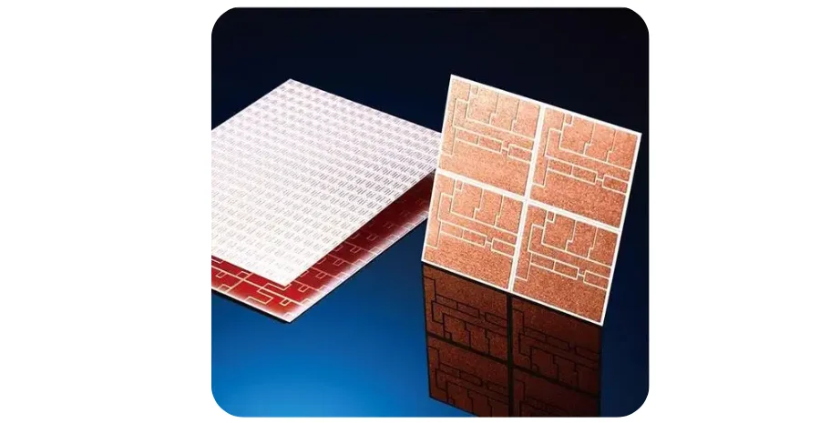
Ceramic circuit boards are engineered for applications that demand high thermal conductivity, electrical insulation, mechanical stability, and long-term reliability under extreme operating conditions. Unlike conventional organic PCB materials, ceramic substrates maintain performance at high temperatures while efficiently transferring heat away from power components.
Highleap PCB Factory (HILPCB) manufactures ceramic circuit boards using alumina (Al2O3), aluminum nitride (AlN), and other advanced ceramic materials for high-power LED modules, power semiconductor packages, RF systems, automotive electronics, and industrial control equipment.
Ceramic PCB manufacturing combines specialized substrate processing, precision metallization, laser machining, and controlled assembly processes. These technologies enable reliable solutions for designs where FR-4 PCB or metal core PCB materials cannot provide sufficient thermal performance or environmental stability.
Advanced Ceramic Materials and Thermal Performance
Ceramic circuit boards use inorganic substrates designed to manage heat, withstand high temperatures, and provide stable electrical insulation. Material selection directly affects thermal performance, dielectric characteristics, mechanical strength, and manufacturing cost.
The most common ceramic PCB materials include alumina, aluminum nitride, beryllium oxide, silicon nitride, and LTCC ceramics.
Alumina (Al2O3) Substrates
Alumina is the most widely used ceramic PCB material because it provides a balance of thermal performance, electrical insulation, mechanical strength, and cost efficiency.
- 96% Al2O3: Standard ceramic substrate with 24-28 W/m·K thermal conductivity
- 99.6% Al2O3: High-purity ceramic with improved electrical insulation and mechanical properties
- Thermal expansion coefficient: 6.5-7.5 ppm/K, compatible with many silicon semiconductor devices
- Maximum operating temperature: 1500°C in inert atmosphere
Alumina substrates are commonly used in LED packages, thick film circuits, sensors, power modules, and industrial electronics.
Aluminum Nitride (AlN) Solutions
Aluminum nitride provides significantly higher thermal conductivity than alumina while maintaining electrical insulation. It is preferred for applications that generate large amounts of heat in compact designs.
- Thermal conductivity: 170-230 W/m·K
- Low dielectric constant: 8.8 at 1 MHz
- Thermal expansion coefficient: 4.5 ppm/K, closely matching semiconductor materials
- Suitable for high-power RF amplifiers, laser diodes, IGBT modules, and SiC/GaN power devices
AlN ceramic substrates reduce thermal resistance between semiconductor junctions and cooling structures, improving system efficiency and reliability.
Specialized Ceramic Options
For specialized applications, HILPCB supports additional ceramic material technologies:
- Beryllium Oxide (BeO): Provides approximately 280 W/m·K thermal conductivity but requires strict handling procedures due to material safety considerations
- Silicon Nitride (Si3N4): Offers higher fracture toughness and excellent thermal cycling performance
- LTCC (Low Temperature Co-fired Ceramic): Enables multilayer ceramic circuits with embedded components, cavities, and three-dimensional interconnect structures
Ceramic substrates provide advantages including zero moisture absorption, chemical resistance, high dimensional stability, and reliable dielectric performance at elevated temperatures. These characteristics make ceramic PCBs suitable for environments where conventional PCB materials experience thermal expansion, degradation, or heat dissipation limitations.
Metallization Technologies for Ceramic Circuit Boards
Ceramic materials require specialized metallization processes because standard copper etching methods used for organic PCBs are not directly applicable. The metallization method determines conductor thickness, current capability, frequency performance, and assembly compatibility.
HILPCB supports multiple ceramic metallization technologies based on application requirements.
Direct Bonded Copper (DBC)
Direct bonded copper technology creates a strong copper-to-ceramic connection by bonding copper foil directly to the ceramic surface at high temperatures.
Key DBC characteristics include:
- Copper foil thickness options from 127μm to 400μm
- High-temperature bonding process at approximately 1065°C forming a Cu-O eutectic bond
- Current carrying capability exceeding 100A per trace depending on design parameters
- Thermal cycling reliability from -55°C to +150°C for more than 1000 cycles
DBC ceramic substrates are widely used in power semiconductor modules, electric vehicle systems, renewable energy converters, and industrial power electronics.
Thick Film Technology
Thick film ceramic PCB manufacturing uses screen printing processes to deposit conductive pastes onto ceramic surfaces.
Typical materials include:
- Silver (Ag)
- Gold (Au)
- Copper (Cu)
- Silver-palladium (AgPd)
Capabilities include:
- Fine line structures with 75μm traces and 75μm spacing
- Multilayer circuit structures with via interconnections
- Embedded resistors and capacitors for integrated passive components
Thick film technology provides a cost-effective solution for ceramic circuits requiring high reliability and moderate feature sizes.
Thin Film Processing
Thin film ceramic circuits use sputtering or evaporation processes to create highly precise conductor patterns.
Advantages include:
- Line and space capability down to 10μm
- Excellent performance for microwave and high-frequency circuits
- Compatibility with wire bonding and flip-chip assembly
- High-density interconnect capability
HILPCB maintains Class 1000 cleanroom environments for thin film processing to control contamination during precision metallization.
Manufacturing Excellence for Ceramic PCB Production
Ceramic PCB manufacturing requires specialized equipment because ceramic substrates are harder and more brittle than conventional PCB laminates. HILPCB combines precision processing equipment with controlled manufacturing procedures to maintain dimensional accuracy and reliability.
Laser Processing Systems
Laser processing enables accurate drilling, cutting, and separation of ceramic substrates without introducing mechanical stress.
Capabilities include:
- CO2 and UV laser drilling for ceramic vias
- Precision singulation for finished substrates
- Laser scribing for controlled fracture separation
- Minimum via diameter: 50μm with ±10μm tolerance
Laser machining improves yield and reduces the risk of cracking during ceramic substrate processing.
Quality Control Infrastructure
Ceramic PCB reliability depends on strict inspection throughout manufacturing. HILPCB applies multiple inspection methods, including:
- Automated optical inspection with 0.5μm resolution
- X-ray inspection for hidden defects and internal structures
- Coordinate measuring machines for dimensional verification
- Thermal impedance testing for heat transfer validation
These inspection processes verify conductor accuracy, substrate integrity, and thermal performance before shipment.
Production Capabilities
HILPCB ceramic PCB manufacturing supports:
- Panel sizes up to 200mm x 200mm
- Ceramic thickness range from 0.25mm to 3.0mm
- Single-sided, double-sided, and multilayer ceramic configurations
- Monthly production capacity exceeding 50,000 ceramic substrates
Standard ceramic PCB prototypes can be delivered within 7-10 days for qualified designs. Automated handling systems support scalable production while minimizing damage risks associated with brittle ceramic materials.
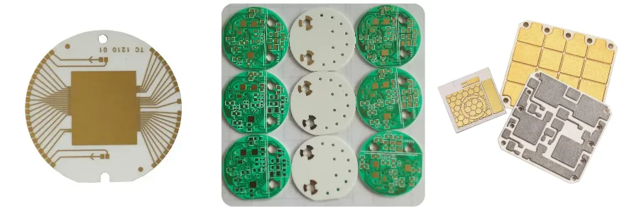
Thermal Management Solutions Using Ceramic Substrates
Ceramic circuit boards are selected when thermal performance directly affects product reliability, efficiency, and operating life. Their high thermal conductivity allows heat to move away from power devices more efficiently than conventional PCB materials.
For high-power LED applications, ceramic substrates provide a direct thermal path from LED dies to the heat dissipation structure. HILPCB ceramic solutions support:
- Junction-to-board thermal resistance as low as 0.5 °C/W
- Direct die attachment without additional thermal interface layers
- More than 50,000 hours of reliable operation at junction temperatures of 150 °C
- Phosphor deposition capability for integrated white LED applications
In power electronics, ceramic PCBs support advanced semiconductor packaging requirements, including:
- IGBT modules with integrated gate drivers
- Silicon carbide (SiC) power devices
- Gallium nitride (GaN) devices
- High-current power conversion systems
Ceramic substrates improve thermal spreading and can provide thermal performance improvements up to 10 times greater than standard FR-4 materials in suitable designs. Metallized microchannel structures can also support direct liquid cooling solutions for high-power applications.
To optimize thermal performance before production, HILPCB provides finite element analysis (FEA) simulation services. Engineers analyze copper distribution, component placement, thermal paths, and mechanical stress conditions to improve heat dissipation and reduce thermal failure risks.
Assembly Services for Ceramic Circuit Boards
Ceramic circuit board assembly requires different process controls compared with standard PCB assembly. Ceramic materials have high thermal conductivity but are also brittle, requiring careful handling during soldering and component placement.
HILPCB provides specialized SMT assembly services designed for ceramic substrates.
Process Adaptations
Ceramic PCB assembly includes:
- Controlled preheating profiles to prevent thermal shock
- Specialized fixtures to support brittle ceramic materials
- Lead-free soldering with controlled cooling rates
- Gold or aluminum wire bonding processes
Component Attachment Methods
Depending on thermal and mechanical requirements, ceramic assemblies can use:
- Conductive epoxy for stress-sensitive components
- Eutectic die attachment for improved thermal transfer
- Flip-chip assembly with underfill dispensing
- Silver sintering for extreme-temperature applications
Our turnkey assembly services include component sourcing, programming, and functional testing to deliver complete ceramic circuit board assemblies ready for system integration.
Global Delivery and Customer Support Excellence
HILPCB supports customers throughout ceramic PCB development, from material selection and prototype design to production delivery.
Our engineering support includes ceramic substrate selection, thermal analysis, manufacturability review, and design optimization. A DFM review identifies potential issues related to ceramic brittleness, conductor layout, thermal stress, and assembly requirements before production begins.
For global customers, HILPCB provides packaging methods designed specifically for ceramic substrates. Shock-resistant materials help protect finished boards during transportation.
Quality documentation includes:
- 100% electrical testing according to customer specifications
- Dimensional inspection reports
- Material certificates verifying ceramic composition and properties
- Serialization and manufacturing traceability records
- RoHS compliance documentation
After delivery, HILPCB continues to support customers with assembly guidance, troubleshooting assistance, and design improvements based on application feedback.
FAQ
What are the main advantages of ceramic circuit boards over traditional PCBs?
Ceramic circuit boards provide significantly higher thermal conductivity than FR-4 PCBs, allowing efficient heat removal in high-power applications. They also offer low moisture absorption, stable dimensions at elevated temperatures, strong electrical insulation, and reliable performance at high frequencies. These characteristics make ceramic PCBs suitable for power electronics, RF systems, LED modules, and automotive applications.
How do ceramic PCB costs compare to standard circuit boards?
Ceramic substrates typically cost 3-10 times more than equivalent FR-4 boards because they require specialized materials and manufacturing processes. However, ceramic PCBs can reduce total system costs by improving reliability, reducing cooling requirements, eliminating additional heatsinks in some designs, and extending product operating life.
Can ceramic circuit boards be manufactured in multilayer configurations?
Yes. HILPCB supports multilayer ceramic circuit manufacturing using LTCC technology with up to 20 layers. LTCC enables three-dimensional circuit integration, embedded passive components, cavities, and internal channels. Standard alumina and AlN substrates are typically used for single-sided, double-sided, or thick film multilayer structures.
What design rules apply to ceramic circuit board layouts?
Ceramic PCB layouts require design rules based on material type and metallization process. Typical guidelines include:
- Minimum trace width: 100μm for thick film processes and 10μm for thin film processes
- Via diameters starting at approximately 100μm depending on technology
- Edge clearance requirements to reduce ceramic chipping risk
- Thermal expansion considerations between ceramic substrates and attached components
HILPCB provides ceramic PCB design guidelines based on the selected material, metallization process, and assembly method.
How quickly can you deliver ceramic circuit board prototypes?
Standard ceramic PCB prototypes can be delivered within 7-10 business days for single-sided and double-sided designs. Complex LTCC multilayer structures or custom metallization processes may require 15-20 business days. Prototype timelines depend on material availability, design complexity, and testing requirements.
What certifications do you hold for ceramic PCB manufacturing?
HILPCB maintains ISO 9001:2015 quality certification, IATF 16949 certification for automotive applications, and AS9100D certification for aerospace manufacturing. Ceramic PCB processes follow applicable IPC standards adapted for ceramic substrates. We provide material traceability, RoHS compliance documentation, and customized testing reports based on customer requirements.