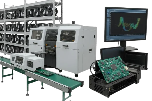
In the field of renewable energy inverters, PCBs are no longer just carriers for components but also the core of energy conversion, precision control, and high-voltage safety. To ensure that every PCB leaving the factory operates stably under harsh conditions, comprehensive and precise testing is crucial. This is where Fixture Design (ICT/FCT) plays a pivotal role. An excellent test fixture design is not only a quality sentinel on the production line but also a bridge connecting design verification and mass production, running through the entire NPI EVT/DVT/PVT process to ensure the inverter meets the highest standards in efficiency, reliability, and safety.
The Core of Fixture Design (ICT/FCT): Ensuring MPPT Sampling Accuracy and Consistency
Maximum Power Point Tracking (MPPT) is the soul of photovoltaic inverters, and its efficiency directly depends on real-time, accurate sampling of the photovoltaic array's voltage and current. Any sampling error can lead to significant power output loss. Therefore, the primary task of Fixture Design (ICT/FCT) is to precisely verify the performance of these critical analog sampling circuits.
The test fixture must provide an "electromagnetically clean" environment. Through careful probe layout, shielding, and grounding design, it avoids introducing additional noise during testing, thereby accurately evaluating the true signal-to-noise ratio and effective resolution of the sampling circuit. Before functional testing, methods such as SPI/AOI/X-Ray inspection can preemptively detect soldering defects or component misplacement, preventing these basic errors from interfering with subsequent complex electrical performance verification. Throughout the NPI EVT/DVT/PVT stages, ICT/FCT test data provides critical insights for design iterations, ensuring the final product's consistency and reliability.
High-Voltage Isolation Testing Challenges: How to Verify Common-Mode Rejection and Bandwidth Performance?
Inverters internally contain both high-voltage DC buses and low-voltage control circuits, with isolation between them being a top priority for safety regulations. Isolated amplifiers and optocouplers are key components for signal isolation, and their common-mode rejection ratio (CMRR) and signal bandwidth directly impact the stability and dynamic response of the control loop.
In Fixture Design (ICT/FCT), testing these isolation channels is highly challenging. The fixture must:
- Safely apply high common-mode voltage: The test fixture must integrate a high-voltage source and feature robust insulation and safety interlock mechanisms to simulate high common-mode voltage surges under real operating conditions.
- Precisely measure weak differential signals: Capturing microvolt-level differential signals under strong common-mode interference places extremely high demands on the fixture's signal integrity design.
- Evaluate dynamic performance: By injecting swept-frequency signals, verify the gain and phase characteristics of the isolation channels across different frequencies to ensure they meet the control system's required bandwidth.
The success of this process relies on high-quality SMT Assembly, which ensures the soldering reliability of isolation components and avoids performance degradation due to cold solder joints or misalignment. For PCBs operating under high temperatures and voltages, using High-Tg PCB materials can significantly enhance long-term reliability.
Key Reminder: Critical Aspects of High-Voltage Isolation Testing
- Safety First: The fixture must have comprehensive high-voltage protection and interlock designs to safeguard both operators and the device under test.
- Signal Integrity: Test probes, cables, and switching relays must be carefully selected and laid out to minimize signal attenuation and crosstalk.
- Automated Calibration: Integrate automated calibration procedures to periodically compensate for test system drift, ensuring long-term measurement consistency.
- Thermal Management: For modules requiring load testing, the fixture should incorporate cooling systems to simulate real-world operating temperatures.
Precision Sampling Network Testing: Addressing Thermal Drift and Tolerance in Voltage Divider/Shunt Circuits
In addition to active isolation amplifiers, voltage divider networks (Divider) composed of precision resistors and shunts (Shunt) made of alloys like constantan or manganin are common solutions for voltage and current sampling. The accuracy, temperature drift, and long-term stability of these passive components directly determine measurement reliability.
During the ICT (In-Circuit Test) phase, the fixture's "bed of nails" can precisely access test points on these networks to measure the exact resistance of each resistor, screening out PCBA units that exceed tolerance limits. In the FCT (Functional Circuit Test) phase, system-level calibration of the entire sampling chain is required. Using Boundary-Scan/JTAG technology, the test system can communicate directly with the main MCU, read ADC sampling values, and compare them with reference voltage/current provided by high-precision source meters on the fixture to calculate calibration coefficients for each PCBA. This not only validates hardware design but also completes a critical calibration step in production. For high-current shunts, employing Heavy Copper PCB technology effectively reduces temperature rise and enhances measurement stability.
High-Voltage Hipot and Bandwidth Testing (Example)
| Item | Typical Practice/Range (Example) | Key Points |
|---|---|---|
| Hipot (Withstand Voltage/Leakage) | DC 1–3 kV; Leakage at μA level | Creepage/clearance with selective coating, MES recording curve |
| Isolation channel bandwidth | Sweep frequency injection, measure gain/phase | CMRR/frequency response matching control loop requirements |
Note: Parameters are generic examples; actual values should comply with applicable standards and product safety/performance objectives. It is recommended to finalize them in SOP/MES during the FAI stage.
Test Coverage Matrix (Object × Method)
| Object/Defect | ICT | FCT | JTAG | Hipot |
|---|---|---|---|---|
| MPPT sampling connectivity/tolerance | ✓ (Bed-of-nails measurement) | — | ✓ (ADC/register area) | — |
| Isolation channel CMRR/bandwidth | — | ✓ (Sweep) | — | ✓ (Withstand Voltage/Leakage) |
Immunity Verification: Simulating ESD/EFT/Surge Impacts in ICT/FCT
Renewable energy inverters typically operate in complex electromagnetic environments and must exhibit excellent immunity to handle transient disturbances such as grid fluctuations, lightning surges (Surge), and electrostatic discharge (ESD). Traditional EMC testing is costly and time-consuming, making it unsuitable for full production line inspection.
An advanced Fixture design (ICT/FCT) can integrate simplified immunity testing to some extent. For example, specialized probes can inject simulated EFT (Electrical Fast Transient) or Surge pulses into critical I/O ports or power rails while monitoring the system's response to detect issues like resets, data errors, or lock-ups. This effectively identifies damaged protective components (e.g., TVS diodes, varistors, etc.) during assembly. These critical through-hole protection components are often assembled using Selective wave soldering to ensure soldering strength and reliability. Meanwhile, the earlier SPI/AOI/X-Ray inspection processes guarantee these components are defect-free during the placement stage.
HILPCB Assembly and Testing Advantages
- One-Stop Service: Offers a complete turnkey solution from PCB manufacturing to component procurement, SMT assembly, and functional testing.
- Advanced Inspection: Integrates SPI/AOI/X-Ray inspection with process data linked to SPC/MES.
- Customized Testing: Engineering team collaborates closely to develop ICT/FCT fixtures and test programs, covering critical scenarios.
- Process Flexibility: Hybrid assembly capability combining SMT + Selective wave soldering, suitable for power and high-voltage components.
Clock and Synchronization Signal Testing: Ensuring Coordinated Sampling and Control
In digitally controlled inverters, the ADC sampling moment must be strictly synchronized with the PWM switching cycle. Any clock jitter or phase offset may lead to control instability. Therefore, testing the board-level clock distribution network and synchronization signals is equally indispensable.
The FCT fixture requires high-speed probes and impedance-matched cables connected to an oscilloscope or high-speed digital analyzer to accurately measure key clock signal parameters such as frequency, duty cycle, and jitter. For complex FPGA or SoC systems, leveraging the Boundary-Scan/JTAG interface not only verifies whether the clock signals correctly reach the chip pins but also enables internal logic self-testing, significantly improving test coverage and efficiency. During the early stages of product development, HILPCB's Small-Batch Assembly service allows for rapid acquisition of high-quality prototypes to validate clock and synchronization schemes.
In summary, Fixture Design (ICT/FCT) serves as the final and most critical line of defense in ensuring the quality, performance, and reliability of renewable energy inverter PCBs. It goes beyond simple "pass/fail" testing, encompassing a comprehensive validation platform that includes analog precision, high-voltage isolation, noise immunity, and high-speed digital signal integrity. A successful test strategy requires close integration of fixture design with PCB design, SMT Assembly processes, and process control measures such as SPI/AOI/X-Ray Inspection. As your reliable partner, HILPCB leverages deep engineering expertise and advanced manufacturing capabilities to provide end-to-end support from design to mass production, ensuring your product stands out in a competitive market.