
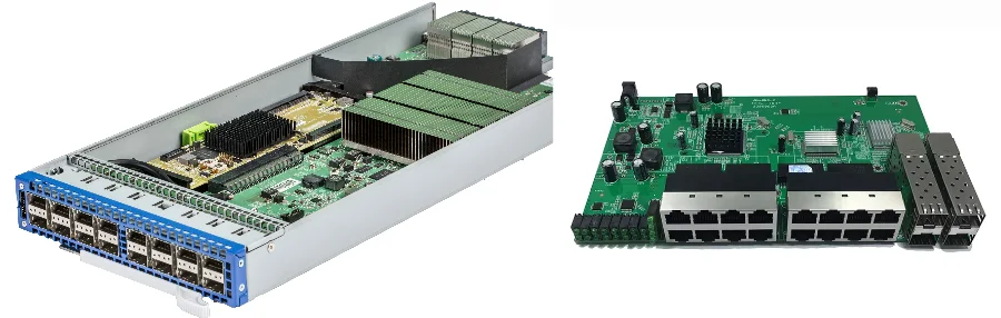
As a safety control engineer focused on dual-channel safety, E-Stop, and watchdog mechanisms, I know that in industrial automation—especially robotics PCB control—performance and safety must advance together. high-speed EtherCAT interface PCB is a concentrated expression of that principle. It must carry the real-time data stream enabled by EtherCAT at 100M and even 1G bitrates, while serving as the physical foundation of functional safety to ensure protective functions execute reliably under all conditions. This article, from a safety engineer’s perspective, explains the key challenges and design strategies for building an EtherCAT interface board that is both fast and safe.
EtherCAT (Ethernet for Control Automation Technology) has become the preferred fieldbus for high-performance motion control thanks to excellent real-time behavior, precise synchronization, and flexible topologies. However, once you integrate safety functions (e.g., STO, SS1) into EtherCAT-based drives or I/O modules, PCB requirements grow exponentially. This is not only about high-speed SI; it is about achieving the SIL/PL targets required by IEC 61508 or ISO 13849 through hardware design. A successful high-speed EtherCAT interface PCB must balance two seemingly conflicting objectives: high-speed communication and functional safety. That demands holistic design—from architecture and placement to manufacturing processes.
SIL/PL target decomposition and hardware architecture trade-offs
For any safety-related control system, the first task is to determine the required SIL or PL. The target level dictates architecture complexity and redundancy. For high-speed EtherCAT interface PCB, that means decomposing system-level targets (e.g., PLd or SIL 2) into concrete hardware requirements.
HFT and architecture selection
Under IEC 61508 and ISO 13849, architecture is the foundation of achieving SIL/PL. Common architectures include:
- 1oo1 (1-out-of-1): single-channel. Simple and low cost, but heavily dependent on diagnostics; hard to reach higher SIL/PL using only 1oo1.
- 1oo2 (1-out-of-2): dual-channel redundancy. If one channel fails, the system transitions to a safe state; commonly used for PLd/SIL 2 and above.
- 2oo2 (2-out-of-2): dual-channel where both must be OK to run; used where availability is prioritized.
For industrial robot safety control, 1oo2 is most common. At PCB level, this means designing two physically independent and electrically isolated processing channels for safety-related signals (E-Stop inputs, encoder feedback, motor enable outputs). This directly impacts placement, routing, and layer count, often requiring multilayer PCB to achieve effective channel isolation.
Quantifying MTTFd, DC, and CCF
After selecting the architecture, you validate targets via quantitative parameters:
- MTTFd: strongly related to component reliability. PCB design should choose certified/high-reliability components and use appropriate derating.
- DC (Diagnostic Coverage): achieved via cross-monitoring, periodic self-tests, and test pulses—requiring dedicated circuits and routing.
- CCF (Common Cause Failures): preventing a single event from defeating both channels is critical. PCB measures include:
- Physical separation: keep channel components/routing far apart.
- Electrical isolation: use optocouplers or safety relays between domains.
- Diversity: different technologies or vendors per channel (at higher complexity/cost).
A good EtherCAT interface PCB guide emphasizes making these trade-offs early, because they also determine EtherCAT interface PCB cost optimization. At HILPCB, we help customers evaluate options early to find the best balance of safety, cost, and performance.
Dual-channel safety: achieving DC with diagnostics and periodic tests
With a 1oo2 architecture, design focus shifts to effective monitoring and diagnosis between channels to reach high DC. On high-speed EtherCAT interface PCB, this means carefully designing diagnostic circuits around MCU/FPGA.
Cross-monitoring
Cross-monitoring is the core diagnostic technique in dual-channel systems. Two independent MCU (or a lockstep dual-core MCU) process safety signals and monitor each other in real time.
- State comparison: exchange and compare key state information (input states, computed results, output drive states). Any mismatch is treated as a fault.
- Timing monitoring: one MCU monitors whether the other feeds the watchdog or sends a heartbeat within the expected window. Timing anomalies are also faults.
PCB implementation requires:
- Dedicated communication lines: robust links such as SPI or UART between MCUs, with sufficient signal integrity.
- Avoid new single points of failure: ensure the monitoring path itself is diagnosable (short/open detection).
- Physical isolation: keep channels physically separated to mitigate CCF. During EtherCAT interface PCB manufacturing, measures like milling slots can increase creepage/clearance.
Periodic self-tests and test pulses
To detect “hidden” faults that don’t appear during normal operation (e.g., an output driver stuck ON), periodic self-tests are required.
- Input tests: periodically simulate input transitions and verify both channels respond correctly.
- Output test pulses: a common method to diagnose output stages (MOSFET/IGBT). The system sends a very short OFF pulse (typically microseconds). It is too short to move the motor/actuator macroscopically, but long enough for feedback to detect a transient voltage change. If the change is not detected, the output stage may be stuck.
Implementing test pulses on high-speed EtherCAT interface PCB requires careful layout. The feedback loop must be fast and low-noise to capture microsecond pulses reliably, and the pulses must not interfere with high-speed EtherCAT communication or sensitive analog circuits.
Table 1: single-channel vs dual-channel safety architecture
| Attribute | Single-channel (1oo1) | Dual-channel (1oo2) |
|---|---|---|
| Achievable safety level | Typically up to PLc / SIL 1 | Up to PLe / SIL 3 |
| Hardware redundancy | None; relies on diagnostics | Yes; tolerance via redundant channels |
| DC requirement | Higher (DC=medium) to raise level | High DC (≥90%) easier via cross-monitoring |
| CCF resilience | N/A (no redundancy) | Key design point; ensure via physical/electrical isolation |
| PCB design complexity | Lower | High; strict isolation and symmetric placement |
| Cost | Low | Higher |
E-Stop loop: debouncing, redundancy, and fail-safe design
The E-Stop loop is the most critical part of any machine safety system. On high-speed EtherCAT interface PCB, E-Stop input processing must follow strict fail-safe principles.
Redundant inputs and wire-break detection
A compliant E-Stop loop typically uses dual-channel NC contacts. In normal state, both loops are closed; pressing E-Stop opens both loops. The safety MCU monitors both input channels.
- Redundancy: the system confirms E-Stop only when both channels open. If only one opens, it is treated as a fault (loose wiring/contact failure) and the system enters a safe state.
- Fail-safe by NC contacts: common faults like cable break or connector disengagement mimic an E-Stop press, stopping the system rather than allowing unsafe operation.
PCB design should provide independent pull-up/pull-down and filtering circuits for both channels, and keep routing separated.
Hardware debouncing and signal robustness
Mechanical switches bounce at millisecond scale. Without handling, MCU may detect multiple toggles, causing abnormal behavior.
- Hardware debouncing: RC filtering is common. RC time constant is a trade-off: too small doesn’t debounce; too large increases E-Stop response time.
- Signal robustness: although E-Stop is “low speed”, reliability is critical. On complex high-speed EtherCAT interface PCB, high-speed digital signals can couple noise into E-Stop traces. Shielding, robust routing practices, and disciplined EtherCAT interface PCB impedance control (not for high-speed matching here, but for noise immunity and controlled electrical behavior) all matter. HILPCB’s Impedance Calculator helps engineers control electrical characteristics of critical nets.
Comprehensive EtherCAT interface PCB testing must include detailed E-Stop validation, simulating faults (single-channel open/short) and response under worst-case EMI environments.
Watchdog / test pulses: fault detection and fault reaction time
Watchdogs and test pulses are two key techniques for active fault detection and directly determine Fault Reaction Time (FRT).
Independent external watchdog
For safety systems, MCU internal watchdog alone is insufficient (it may not detect MCU clock failures and other CCF). Robust designs should use an independent external watchdog IC.
- Windowed watchdog: requires feeding within a defined time window; feeding too early or too late triggers reset—detecting runaway code or stuck loops.
- Independent clock: external watchdog should use a different clock source than the main MCU so it remains functional even if the main clock fails.
In PCB placement, treat the watchdog circuit as a key safety element: keep its power/ground clean and away from noise sources. A detailed EtherCAT interface PCB guide will recommend driving the final safety output enable directly from watchdog reset, creating a protective layer independent of the main processor.
Fault Reaction Time (FRT) composition
FRT is the maximum allowed time from fault occurrence to reaching a safe state. It consists of:
- Detection time: time for diagnostics (cross-monitoring, self-test) to detect the fault.
- Decision time: time for MCU or safety logic to process and decide.
- Reaction time: time for the output stage to shut down (e.g., cut motor power).
The entire high-speed EtherCAT interface PCB must be designed to minimize FRT: fast optocouplers, fast relays, and optimized software. In certification, FRT must be measured and verified.
🛡️ Closed-loop fault diagnostics and safety reaction timing (FDT/FRT)
Hardware failure (e.g., MOSFET short or stuck) pushes the system into an unsafe undetected state.
Periodic diagnostic pulses or read-back circuits detect anomalies and set fault flags.
Safety MCU performs dual-core checks, evaluates risk per safety strategy, and issues a shutdown command.
Activate STO or drop the relay so the system returns to a controlled safe state.
Safety relays / optocouplers: lifetime, reliability, and manufacturability
In safety output circuits, safety relays and optocouplers are core components for electrical isolation and reliable switching. Their selection and use directly impact long-term reliability and manufacturability.
Safety relays and forcibly guided contacts
Safety relays differ from ordinary relays via forcibly guided (mechanically linked) contacts.
- How it works: internal NO and NC contacts are mechanically linked. If an NO contact welds and cannot open, the corresponding NC cannot close.
- Diagnostics: by monitoring the NC status, the safety system can infer the NO status. If the relay is commanded open but NC does not close, the main circuit may not be safely cut, so the system alarms and blocks restart.
On PCB, safety relays are usually large, through-hole devices. In EtherCAT interface PCB manufacturing, reliable Through-hole Assembly is required to ensure solder quality. Also, relay coils generate EMI; place relays away from sensitive analog and high-speed digital routes.
Safety optocouplers and isolation considerations
Optocouplers provide isolation between safety logic and high-voltage outputs (or noisy inputs). For safety applications, choose optocouplers compliant with standards like VDE 0884-11 with reinforced insulation.
- Aging: CTR degrades over time and temperature. Design must consider worst-case CTR and include sufficient margin for lifecycle operation.
- Creepage/clearance: PCB layout must meet safety creepage and clearance requirements. This often means milling slots between optocoupler input and output to increase surface insulation distance.
EtherCAT interface PCB cost optimization here means selecting safety components with best value and stable supply while meeting certification requirements. Final EtherCAT interface PCB testing must include Hi-pot test to verify the isolation barrier.
Conclusion
Building a high-performance, high-reliability high-speed EtherCAT interface PCB is a complex task integrating high-speed digital design, power management, and functional safety engineering. As safety control engineers, we care not only about EtherCAT throughput and stability, but the determinism and reliability of every embedded safety function. From SIL/PL decomposition, to dual-channel implementation, to detailed E-Stop and watchdog design—every step involves trade-offs.
The design must treat DC, FRT, and CCF as core metrics. This means PCB design is not merely interconnect—it becomes an “intelligent” hardware platform that can detect its own faults and transition to a safe state. Partnering with an experienced manufacturer like HILPCB is crucial: beyond high-quality high-speed PCB fabrication, HILPCB provides DFM feedback in Prototype Assembly to ensure safety designs land correctly and ultimately pass strict functional safety certification.
Common Questions
Why is dual-channel architecture common in EtherCAT safety interface PCBs?
Because dual-channel architecture helps the board reach higher SIL or PL targets by adding redundancy and cross-monitoring. It allows one channel to detect faults in the other and supports safe-state transitions when abnormal behavior is found.
What safety metrics matter most in high-speed EtherCAT interface PCB design?
Design teams usually focus on DC, FRT, CCF, and the system’s target SIL or PL. These metrics determine not only the logic architecture, but also isolation strategy, diagnostics, spacing, and manufacturability requirements on the PCB.
Why must EtherCAT safety boards include Hi-pot and isolation verification?
The board often separates hazardous and safe domains while carrying safety-related control signals. Hi-pot and isolation checks confirm that creepage, clearance, and insulation barriers remain effective under real production conditions.
What should be validated before volume production of an EtherCAT interface PCB?
Teams should validate signal integrity, watchdog and test-pulse behavior, channel diagnostics, safety relay or optocoupler implementation, and isolation robustness. Functional safety hardware cannot rely on communication performance alone.