
High-Speed PCB Manufacturing | 25–112 Gbps | PCIe Gen5/Gen6 | Impedance ±5%
High-speed digital PCBs for PAM4/NRZ channels: 25–112 Gbps SerDes, PCIe Gen5/Gen6, back-drilling, low-loss and ultra-low-loss stackups, and controlled impedance ±5% verified by TDR/VNA. Seven-day quick-turn prototypes.
Capabilities
Channel Optimization and Loss Budget Management
Engineer PAM4/NRZ channels for maximum eye height and BER marginOnce rise time drops below 100–200 ps or data rate exceeds 10 Gbps, interconnect behavior dominates overall system performance. Our high-speed design focuses on three pillars: insertion loss (material Df 0.001–0.004), impedance control (target tolerance ±5%), and power distribution network (PDN) impedance. Using controlled impedance design and residual stub removal through back-drilling, we maintain open eye height and controlled jitter to meet CTLE/DFE equalization budgets and BER targets as low as 10⁻¹² (one error per trillion bits).
Material selection aligns to both loss budget and signal reach. For example, Megtron 6 (Df ≈0.002 — at 10 GHz) supports 28 Gbps NRZ over 12–15 inches.
Tachyon 100G and Isola I-Speed with low-roughness copper extend 56–112 Gbps PAM4 channels to 20–25 inches. Low-profile copper (Ra ≤1.5 μm) reduces insertion loss by 3–8% compared to standard foils. For dielectric optimization, see our high-frequency materials guide and HDI PCB stackup options.
Critical Risk: Poor via transitions, uncontrolled reference plane changes, or fiber-weave effects can lead to skew, mode conversion, and eye closure beyond recovery capability. Inconsistent plating thickness also increases via stub resonance and return loss, degrading channel compliance.
Our Solution: We apply signal integrity simulation using S-parameter and 3D field solvers for pre-layout validation. Via optimization is verified through back-drilling and TDR/VNA correlation to ensure impedance variation remains within ±3%. Each design undergoes time-domain reflection (TDR) and eye diagram validation per IEEE 802.3/CEI compliance. For ultra-long reach or mixed-signal systems, hybrid builds combining backplane PCBs and high-frequency PCBs achieve balanced signal integrity and thermal control.
- Differential impedance 85/90/100 Ω ±5% verified by TDR
- Material Df 0.001–0.004 @10 GHz
- Back-drilling residual stub <10 mil for 56 Gbps and above
- Fiber-weave skew mitigation: ±7° routing or spread-glass
- PDN target impedance modeling to meet transient current
- Pair length tolerance ≤5–10 mil
🚀 Quick Quote Request
📋 Get Full Capabilities
Deterministic Manufacturing for Repeatable S-Parameters
Statistical process control and registration accuracy for lot-to-lot consistencyWe hold production impedance variation within ±5% by compensating dielectric thickness and trace width. LDI controls trace width to ±10% of nominal; interlayer registration remains within ±25–50 μm. Multi-depth back-drilling delivers residual stubs <10–15 mil for 25–28 Gbps; 112 Gbps targets ~5 mil.
Sequential lamination supports hybrid stackups (ultra/low-loss where it matters, FR-4 elsewhere), reducing material cost by 30–50% while preserving channel budgets. Resin flow control prevents glass exposure that could shift local Dk. See HF/HS manufacturing flow. For heavy power-distribution layers within the same design, evaluate our heavy copper PCB capabilities for PDN robustness.
- LDI trace-width control ±10%
- Multi-depth back-drilling with cross-section verification
- Hybrid stackups: ultra-low-loss plus standard materials
- Layer-to-layer registration ±25–50 μm
- Low-roughness copper adhesion with oxide alternatives
High-Speed Digital PCB Technical Specifications
Optimized for 10 Gbps NRZ through 112 Gbps PAM4
| Parameter | Standard Capability | Advanced Capability | Standard |
|---|---|---|---|
Layer Count | 2–20 layers | Up to 48 layers | IPC-2221 |
Base Materials | Isola I-Speed, RO4350B | Megtron 6/7, Tachyon 100G, PTFE | IPC-4103 |
Board Thickness | 0.8–2.4 mm | 0.4–5.0 mm (±5%) | IPC-A-600 |
Copper Weight | 0.5–2 oz | Up to 5 oz (PDN layers) | IPC-4562 |
Min Trace/Space | 75/75 μm (3/3 mil) | 50/50 μm (2/2 mil) | IPC-2221 |
Dielectric Constant (Dk) | 3.0–4.5 | <3.0 (PTFE-class) | Material datasheet |
Loss Tangent (Df) | <0.005 @10 GHz | ≤0.002 @10 GHz | Material datasheet |
Impedance Control | ±10% | ±5% (learn more) | IPC-2141 |
Surface Finish | ENIG, Immersion Silver | ENEPIG, Soft/Hard Gold | IPC-4552/4556 |
Quality Testing | TDR, AOI, E-Test | VNA, Eye Diagram, Jitter | IPC-9252 |
Certifications | ISO 9001, UL, IPC Class 3 | IATF 16949, AS9100 | Industry standards |
Lead Time | 7–15 days | Five-day expedite | Production schedule |
Ready to start your PCB project?
Whether you need simple prototypes or complex production runs, our advanced manufacturing capabilities ensure excellent quality and reliability. Get your quote within 30 minutes.
Differential Routing and Reference-Plane Continuity
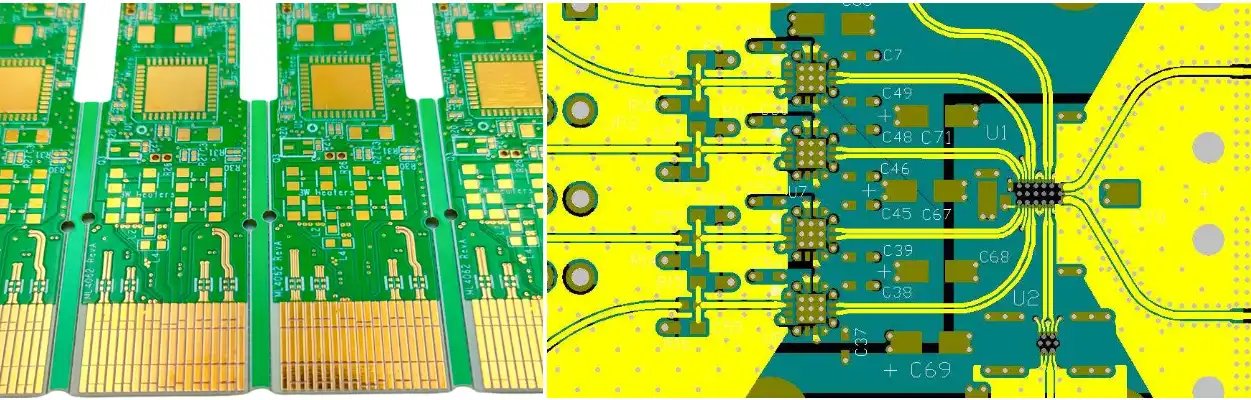
Common targets: PCIe 85 Ω, Ethernet 90 Ω, general 100 Ω. Microstrip is easier to route but radiates more; stripline improves isolation at slight dielectric-loss cost; broadside supports density but requires skew control. Fiber-weave skew is mitigated by ±7° routing or spread-glass fabrics. See high-speed impedance optimization and our complementary high-frequency PCB capabilities for RF domains within mixed systems.
Vias are the dominant discontinuity: tune anti-pads to drill/stackup, place ground-via fences within 0.5–1.0 mm to maintain return paths. Back-drilling removes nonfunctional stubs; at 28 Gbps, residual stubs above ~15 mil can create insertion-loss notches near Nyquist.
Loss Decomposition and Equalization Margin
Above 5–10 GHz, dielectric loss dominates; conductor loss grows with the square root of frequency due to skin effect. Total insertion loss at Nyquist sets equalization needs: beyond 15–20 dB typically requires CTLE plus DFE. Reflections (Sdd11) are commonly targeted better than −10 dB. We use 3D EM to model vias/connectors/AC caps; crosstalk control holds FEXT below −40 dB. See TDR test practice. For tight-bend interconnects between boards or modules, explore our flex PCB options.
Performance Validation and SPC
TDR with 35 ps edge localizes impedance shifts to ±2 mm. VNA measures DC–40 GHz with Sdd21 uncertainty ±0.1 dB. Consistency checks include: copper thickness ±10%, dielectric thickness ±5%, and geometry matched to design targets. Back-drill residual length is confirmed by cross-section. IPC Class 3 workmanship and SPC maintain key Cpk ≥1.33.
AI, Datacom and 5G Use Cases
Data center/AI: 56–112 Gbps line cards and backplane designs, twenty to thirty layers with hybrid stackups; ultra-low-loss only on critical layers; typical channel reach 30–40 inches. PDN target impedance <1 mΩ @100 MHz supports >100 A transients.
5G: 25 Gbps fronthaul coexisting with 28/39 GHz mmWave; partitioned stackups and transitions couple RF and high-speed domains. See 5G PCB technology.
Engineering Assurance & Certifications
Experience: volume programs at 25–112 Gbps with back-drill, blind/buried vias and low-roughness copper.
Expertise: field-solver plus 3D EM for vias/connectors; SPC over impedance/registration/plating; Cpk ≥1.33.
Authoritativeness: IPC-6012 Class 3, IATF 16949, AS9100; audit-ready documentation.
Trustworthiness: MES links lot codes and serialization to TDR/VNA data; lot reports available.
- Process controls: dielectric thickness, registration, copper roughness, back-drill residuals
- Traceability: serialization, lot tracking, digital traveler
- Validation: TDR/VNA, cross-sections, thermal/humidity stress
Frequently Asked Questions
When should I move from FR-4 to low or ultra-low-loss materials?
Back-drilling vs sequential lamination (blind/buried vias): how do I choose?
How do I estimate PDN target impedance?
Can standard FR-4 support 25 Gbps?
How do I mitigate fiber-weave skew?
Which surface finish is best for high-speed?
Experience Advanced PCB Manufacturing Excellence
From simple prototypes to complex production runs, our world-class factory delivers superior quality, fast turnaround and competitive pricing. Join thousands of satisfied customers who trust us with their PCB manufacturing needs.