
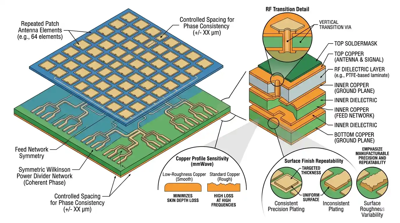
What is the Most Underestimated Engineering Variable in mmWave Antenna Array PCBs
The most underestimated engineering variable in mmWave antenna array PCBs is not nominal low-loss materials, but whether feed network geometry, transition structures, surface states, assembly flatness, and phase consistency can coexist during mass production. For 5G/6G front-ends, beamforming boards, and mmWave modules, what determines pilot production stability is not the simulation curve, but whether these variables can be consistently reproduced by the factory, because the mmWave board itself is part of the RF structure.
Verification Directory
- Why mmWave Array Boards Cannot Just Focus on Low-Loss Materials
- Quick Overview of mmWave Antenna Array PCB Mass Production Review
- mmWave Array Risk and Freeze Item Checklist
- Why Phase Consistency of Feed Networks is More Important Than Nominal Length
- Why Transition Structures, Launches, and Grounding Methods Are the First to Lose Loss Margins
- Why Surface Finishes and Copper States Directly Alter mmWave Results
- Why Thermal, Board Bow, and Mechanical Assembly Amplify Array Dispersion
- How to Establish DFM and Verification Closed Loops for mmWave Array PCBs
- Frequently Asked Questions (FAQ)
- Next Steps: Launching mmWave Array Board Pre-Review and Mass Production Introduction Assessment
Quick Overview of mmWave Antenna Array PCB Mass Production Review
| Risk Dimension | Public Open Information Anchors | Project-level DFM / RF Focus | Engineering Reminders |
|---|---|---|---|
| Band and Link Sensitivity | mmWave designs often involve public band contexts like FR2 and 60 GHz |
Dielectric, copper surfaces, transitions, and assembly variables are significantly amplified in mmWave bands | Small geometric fluctuations are amplified at high frequencies |
| Materials and Stack-ups | Low-loss materials and hybrid structures are common in mmWave boards | Dk/Df stability, dielectric thickness, tolerance chains, and lamination reproducibility must be evaluated together | Material stability is usually more critical than nominal parameters |
| Feed and Transitions | Feedlines, vias, launches, and grounding structures directly affect reflections and phases | Don't just look at nominal length; evaluate geometric consistency and manufacturability | Feed transitions must be evaluated based on mass production geometric consistency |
| Assembly and Verification | Active front-ends, shielding, and mechanical fixation affect RF stability | Flatness, grounding contact, thermal, and batch-to-batch retesting should be included in verification matrices | RF verification focus is on batch consistency, not single-board performance |
mmWave Array Risk and Freeze Item Checklist
| Most Vulnerable Stage | Typical Risks | What to Confirm Before Design Freezing | Late-Stage Costs |
|---|---|---|---|
| Material and Stack-up Definition | Nominal parameters are suitable, but batch stability and lamination reproducibility are inadequate | Material systems, dielectric thickness, tolerances, and hybrid lamination capabilities | Increased dispersion in insertion loss, phase, and radiation patterns |
| Feed Network Definition | Nominal equal lengths are met, but true geometric consistency is inadequate | Branches, bends, tapers, and phase-sensitive structure designs | Beam shifting, channel mismatch |
| Transition and Surface Definition | Launches, vias, and surface states cause additional reflections and losses | Transition geometry, return paths, surface finishes, and copper state | Prototype passible, pilot run drifts |
| Assembly and Verification Release | Shielding, thermal, and fixing structures alter RF results | Flatness, grounding contact, cross-panel/batch retesting matrices | Lengthened debugging cycles, increased rework |
Why mmWave Array Boards Cannot Just Focus on Low-Loss Materials
mmWave array boards cannot just focus on low-loss materials because what determines array performance is never just Df, but whether materials, stack-ups, feed networks, transition structures, surface states, and assembly boundaries hold true together. Even if the nominal material parameters are phenomenal, if dielectric thickness fluctuates, copper states are unstable, or the stress changes significantly after assembly, the array performance will still shift noticeably during the pilot production phase.
In public technical contexts, mmWave boards are often associated with contexts like FR2 covered by 3GPP 38.104 / 38.101-2, 60 GHz wireless systems governed by IEEE 802.11ad, and beamforming modules or high-speed front-end structures. For PCB introduction, what is more critical is:
- Whether material parameters remain stable under batch and temperature changes.
- Whether lamination processes can continuously reproduce target geometries.
- Whether surface conditions and copper profiles have been incorporated into RF reviews.
- Whether the array can still maintain its original phase and loss margins after assembly and shielding.
Therefore, the preliminary freezing goal of mmWave array projects should not just be "materials with low enough loss", but "the entire board-level RF structure can be stably repeated in mass production".
Why Phase Consistency of Feed Networks is More Important Than Nominal Length
The phase consistency of feed networks is more important than nominal length because what mmWave arrays are sensitive to is not the geometric centerline length, but the equivalent electrical length and local phase error of each channel under true manufacturing results. Minor deviations in trace width, bends, branches, taper sections, dielectric thickness, and etch topography will render "nominal equal length" meaningless after the board is manufactured.
What is more worth prioritizing during the design phase is:
- Not only should the lengths of each channel be approximating, but key geometries should also be practically identical.
- Whether bends, branches, and impedance tapers are managed as phase-sensitive structures.
- Whether glass weave styles, local dielectric variations, and copper profiles will amplify phase deviations.
- Whether array critical feedlines are defined based on true manufacturing rules rather than ideal simulation structures.
- Whether there are means to back-annotate phase dispersion into design and engineering files after pilot runs.
Many mmWave projects appear valid in simulation but begin beam deviance during pilot runs; fundamentally, this is usually not because "total length is wrong," but because geometric consistency was not mass-produced. Especially in high-frequency application contexts like 3GPP FR2, whether geometric consistency can be stably duplicated often determines outcomes more than nominal equal length itself.
Why Transition Structures, Launches, and Grounding Methods Are the First to Lose Loss Margins
Transition structures, launches, and grounding methods are the first to lose loss margins because before entering array units, signals often undergo the most sensitive geometric abruptions in connectors, package entry/exits, layer-transitioning vias, and local grounding via arrays. These locations account for little link length, yet are most prone to generating extra reflections, mode conversions, and additional losses.
Mass production-oriented reviews typically should first scrutinize:
- Whether each critical transition point features a continuous, stable return path.
- Whether grounding via arrays surrounding signal vias suffice in suppressing spurious modes.
- Whether anti-pads, local solder mask openings, and reference layer transitions are optimized based on manufacturable structures.
- Whether launch areas factor in real disturbances brought by pads, solder morphologies, and shielding boundaries.
- Whether these localized structures can establish measurement correlation during prototyping and pilot runs.
If the team zeroes in heavily on radiation patterns without initially locking down launches and transitions, signals frequently surrender critical margins prior to ever reaching the array.
Why Surface Finishes and Copper States Directly Alter mmWave Results
Surface finishes and copper states directly alter mmWave results because in mmWave bands, the surface layer and conductor profile are inherently part of the RF path. Rough copper faces, nickel-inclusive surface treatments, stark oxidation gradients, or inter-panel surface inconsistencies will transmute into ancillary losses and batch scattering.
A more reliable pre-emptive review routinely encompasses:
- Whether antenna zones and standard soldering zones dictate divergent surface treatment philosophies.
- Whether the surface treatment has coalesced in review alongside insertion loss objectives, rather than simply being settled by SMT convenience.
- Besides process designations, whether attention is cast on copper profiles and pre-treatment nuances.
- Whether pilot production scopes entail comparing inter-panel and inter-batch surface uniformities.
- Whether local plating, pad clearances, and solder mask boundaries will manipulate key RF zone behaviors.
In low-frequency boards, such inquiries are habitually viewed as secondary; however, in mmWave array boards, they commonly stand as the definitive variables establishing "why golden samples differ from mass production boards". Drawing upon public manufacturing structures like IPC Standards, these deviations invariably must track back to manufacturable geometry, surface states, and batch consistency, not exclusively relying on pure lab sample verdicts.
Why Thermal, Board Bow, and Mechanical Assembly Amplify Array Dispersion
Thermal boundaries, board bowing, and mechanical assemblies amplify array dispersion because, despite the board predominantly negotiating RF, its hardware operation remains subjected to the joint encumbrances of PAs, beamforming chips, shielding cans, thermal interfaces, and bolting structures. Local hot spots, board flatness vacillations, and contact tension adjustments chronically manifest ultimately as impedance mismatching, gain discrepancies, and degenerated uniformities.
What demands joint confirmation prior to design finalization encompasses:
- Whether unyielding, recurrent thermal conduction pathings reside beneath active components.
- Whether copper distribution and layer stack-ups wield sufficient stability to counter board bowing and thermal warping.
- Whether shielding encasements, housing mounts, and thermal structures impinge on cardinal RF zones.
- Whether grounding connectivity and flatness preserve stability post-assembly.
- Whether thermomechanical and RF outcomes merge concurrently into verifications.
If an array board operates seamlessly in bare-board or semi-assembled state but wanders vastly post encasement and thermal attachment, it customarily implicates that geometric boundaries have yet to attain true convergence.
How to Establish DFM and Verification Closed Loops for mmWave Array PCBs
The DFM and verification closed loops for mmWave array PCBs must anchor on "whether RF results can trace back to explicit manufacturing and assembly control items," rather than merely deriving test data from one functional prototype. valuable release conditions aren't just "patterns appearing nominal", but the fact that materials, feedlines, transitions, surfaces, and assembly variances are frozen within the exact same file arrays and verification parameters.
Pragmatic pre-release inspections generally comprise:
- Material and Stack-Up Freeze: Evaluating if material structures, dielectric thicknesses, hybrid-pressing setups, and accomplished copper states stand unambiguously demarcated.
- Feed Network Freeze: Attesting if primary feedlines, tapers, forks, and phase-reactive sections fulfilled mass-production appraisals.
- Transition and Surface Freeze: Resolving if launches, vias, shieldings, treatments, and regional pad perimeters intertwine dynamically with RF intent.
- Assembly and Mechanical Outline Freeze: Assuring if casing, thermal shunting, fastening locations, and planar limits embed tightly into fabrication sets.
- Manufacturing Data Freeze: Ascertaining if compilations conform strictly to system-level PCB Manufacturing Handoff Prerequsites, along with instructions via Design Handoff guidelines, and Gerber Data Preparation Mandates.
- Verification Matrix Freeze: Assessing if S-Parameters, phase consistency, radiating patterns, thermals, and plane deformations interlock dependably into overall Reliability Testing Matrices Procedures.
The strategic yield of this closed loop propels mmWave array boards from "operational within the lab model" into "consistently reproducible after batch introductions," bypassing the perilous deferral of authentic variance hazards into treacherous pilot-ramp climbs.
Frequently Asked Questions (FAQ)
Q: Is designating a low-loss material inherently sufficient for mmWave array boards?
A: Inadequate. Low-loss substrates only represent the baseline tier; elements dominating pilot-scale constancy also demand stringent scrutiny over dielectric tolerances, feed network geometrical consistencies, launch structures, surface parameters, and assembly planar outlines.
Q: Why do mmWave array prototypes frequently pass verification yet meander violently during pilot assemblies?
A: Because mass piloting invariably exacerbates deviations in substrate batches, layer alignments, copper topographical etchings, surface states, cross-shielding contacts, and mechanistic mounting tensions. mmWave models remain highly hypersensitive to such disparities.
Q: Why does the applied surface finish corrupt the mmWave outcomes?
A: Inside mmWave fields, surface stratum states and copper conditions themselves manifest as active RF transmission conduits. Electroless Nickel depositions, harsh copper textures, or cross-panel inconsistencies unreservedly escalate signal hemorrhages and expand batch scattering arrays.
Q: Are array phase uniformities resolved via CAD simulations or via shop floor manufacturing directives?
A: Both intertwine; nonetheless, mass deployment predicates more severely upon production-floor restrictions. Simulation frames the architecture, whereas what legitimately dictates stable replicas remains fixed within geometrical unities, dielectric fidelities, transition designs, and assembly limitations.
Q: What exact components mandate absolute freezing precedence preceding mass escalation runs?
A: Urgently freeze overarching material matrices, key geometries within feed tracts, transfer topologies, surface finish guidelines, physical bolting boundaries, and cross-batch RF analysis metrics. The swifter the freeze, the tighter the yield loops ascend.
Next Steps: Launching mmWave Array Board Pre-Review and Mass Production Introduction Assessment
If your task forces are engaging mmWave array boards, 5G/6G RF modular front-ends, beamforming units, FR2 radio topologies, or identical high-frequency transmission ventures, the potent prelude surpasses questioning "can this be printed?". Instead, amalgamate the accompanying portfolios seamlessly into preliminary audits:
- Stack-up definitions, material stratagems, and critical dialectic tolerance declarations.
- Directives delineating feed networks, transitional via architectures, and apex RF boundaries.
- Mandates outlining surface encasements, guarding partitions, thermal sinkings, and structural assemblies.
- Blueprints charting First Article S-parameters, phase coordinations, and batch recurrence plans.
Cross-verifying these composites abreast 3GPP 38.104 Base Station Guidelines, 3GPP 38.101-2 UE Regulations, the IEEE 802.11ad Protocol Interface, generic IPC Fabrication Standards, and foundational Reliability Testing Procedures Limits precisely determines which metrics conform merely to universal bands, and which necessitate bespoke rigor to govern your precise RF and DFM intents.
If evaluating board architectures, appraising phase symmetry limits, or inaugurating mass-scale DFM pilot protocols ahead of initiating first-articles interests you, promptly Contact the HILPCB Engineering Sector to dissect the project requisites.
Essential Insights for High-Grade DFM Architectures:
- High-Frequency PCB Manufacturing Parameters
- Optimal Blueprints for Design Handoff Architectures
- Critical Directives Encompassing Gerber Data Preparations
- Deploying Systematic Reliability Test Matrices
*Author: HILPCB High-Speed Interconnect Engineering Team* *Reviewed by: HILPCB SI/DFM Engineering Team* *Last Updated: 2026-04-07*