
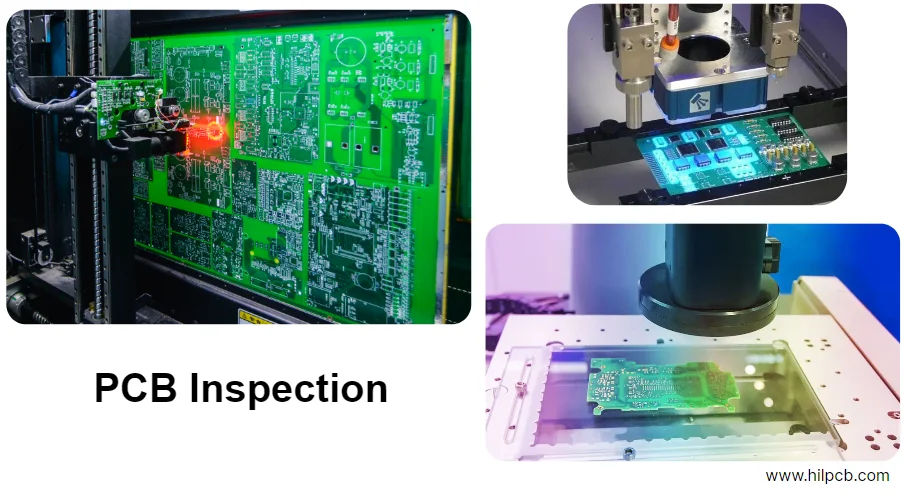
Executive summary: Quality is designed—and manufactured
In high-reliability industries such as automotive electronics, medical devices, industrial automation, and aerospace, a single PCB failure can trigger systemic risk and major commercial loss. Quality is not only a product attribute—it is a systems discipline spanning design, manufacturing, testing, and supply-chain management. At HILPCB, our operating belief is simple: excellent quality comes from precise process control and continuous improvement.
This playbook explains how HILPCB turns quality principles into measurable business outcomes through data-driven manufacturing capability, advanced quality tools, comprehensive test strategy, and end-to-end traceability. We go deep on building and executing a Reliability Test Matrix PCB—not just a test plan, but the core bridge that connects customer requirements, design specs, and manufacturing reality.
Our goal is to achieve and exceed common industry benchmarks:
- Finished-goods FPY (First Pass Yield): > 99.5%
- CPK (Process Capability Index): > 1.67 (6 Sigma level)
- Customer complaint rate (PPM): < 100
With this framework, you’ll see how HILPCB turns targets into repeatable results—so your next high-reliability program ships with a stronger manufacturing and quality foundation.
Manufacturing capability: Precision process is the quality foundation
High-quality PCBs start with tight control at every manufacturing step. From laminate selection to surface finish, HILPCB equips the factory with leading equipment and enforces strict process windows. The table below summarizes key PCB fabrication process steps and capability indicators—the physical basis for reliable products.
HILPCB core manufacturing capability matrix
| Process step | Key capability/parameter | HILPCB specification | High-volume application examples |
|---|---|---|---|
| Lamination | Max layer count / board thickness | 48L / 12mm | Server motherboards, communication backplanes |
| Drilling | Min mechanical / laser via | 0.15mm / 0.075mm | HDI, IC substrate-like designs |
| Imaging/Etching | Min trace / space | 2.5mil / 2.5mil (0.0635mm) | RF modules, medical sensors |
| Solder mask | Solder-mask dam | ≥ 0.05mm | 0.4mm pitch BGA/QFP |
| Surface finish | Finish types | ENIG, ENEPIG, OSP, HASL (Lead-free), Immersion Sn/Ag | Choose by scenario (see DFM checklist) |
| Impedance control | Control accuracy | ±5% (typ.), ±3% (limit) | 5G antennas, high-speed data center |
| Special processes | Blind/buried vias, back-drill, PoP | High aspect ratio (18:1), controlled-depth drilling | Compact electronics, network switches |
| Materials | High-frequency/high-speed laminates | Rogers, Taconic, Isola, Megtron 6/7 | mmWave radar, autonomous-driving ECU |
These numbers are not only capability statements—they are our commitment. Behind every parameter is real-time SPC monitoring to keep production consistently under control.
Quality tools: From data to insight, driving continuous improvement
If manufacturing capability is the skeleton, quality tools are the nervous system. HILPCB’s QMS (quality management system) combines classic statistical methods with modern digital operations to create a closed-loop improvement cycle.
SPC (Statistical Process Control) We monitor critical parameters (e.g., copper thickness, etch rate, lamination temperature) with real-time SPC. Using control charts (X-bar, R-chart), we detect abnormal variation early and intervene before it becomes defects—shifting from “after-the-fact inspection” to “prevention first”.
CPK (Process Capability Index) CPK is the gold standard for whether a process meets its specification. We set CPK > 1.67 as an internal goal—meaning low variation and strong centering—so product consistency and reliability stay high. This is a core indicator of a robust
quality system.MSA (Measurement System Analysis) Data is only as credible as the measurement system. We regularly run Gage R&R studies to ensure AOI, X-Ray, flying-probe testers, and other inspection tools have measurement error far smaller than process tolerances.
8D (Eight Disciplines Problem Solving) When issues occur, we launch a structured 8D workflow: cross-functional team formation, problem definition, containment, root-cause analysis (fishbone, 5-Why), permanent corrective actions, and effectiveness validation—so issues are eliminated and prevented from recurring.
Digital quality dashboards Real-time shop-floor dashboards visualize FPY, equipment OEE, SPC alarms, and other KPIs. This improves management efficiency and makes quality visible to every operator—building a culture of shared accountability.
SMT/assembly capability and defect control
PCB reliability faces new risks during PCBA assembly. HILPCB SMT lines follow IPC-A-610 Class 2/3 standards and use fine-grained process controls to minimize defect rates.
Key process control points
Solder paste printing
- Stencil design (
smt stencil design tutorial): We optimize aperture geometry (aspect ratio, area ratio), stencil thickness, and fabrication process (laser cutting, electropolishing) based on package type and pad size/pitch—so paste release is accurate and consistent. - 3D SPI (Solder Paste Inspection): 100% 3D SPI coverage monitors paste volume, area, height, and offset—preventing soldering defects caused by paste issues (insufficient solder, bridging, cold joints).
- Stencil design (
Reflow soldering
- Profile optimization (
reflow profile basics): We customize a dedicated reflow profile per product. With multi-channel thermocouples, we measure temperatures at multiple PCB locations (e.g., BGA center, mixed-thickness regions) to ensure preheat, soak, reflow, and cooling meet component and paste specs—reducing thermal shock, part damage, and defects like Head-in-Pillow.
- Profile optimization (
Inspection
- Multi-stage AOI (Automated Optical Inspection): AOI before and after reflow detects placement issues (missing, reversed, skew, tombstoning) and solder-joint appearance defects.
- X-Ray inspection (
x ray inspection checklist): For BGA/QFN/LGA bottom-terminated parts, we run 100% 2.5D/3D X-Ray. Ourx ray inspection checklistcovers voiding (<25%), shorts/opens, ball size/shape consistency, and alignment accuracy—ensuring hidden joints are reliable.
Test coverage: Building a complete Reliability Test Matrix PCB
Testing is the final gate for verifying quality, but no single test method guarantees long-term reliability. HILPCB works closely with customers to define a layered, multi-dimensional reliability test matrix based on application, lifecycle, and risk level. This matrix is the blueprint for comprehensive test coverage.
HILPCB reliability test matrix framework
| Stage | Method | Purpose & coverage | Key metrics | Example products |
|---|---|---|---|---|
| Fabrication | E-Test | 100% opens/shorts/net connectivity test. | Netlist match = 100% | All PCBs |
| AOI | Detect trace, solder mask, legend cosmetic defects. | Detection rate > 99% | All PCBs | |
| TDR impedance test | Verify controlled impedance for high-speed nets. | Impedance value/tolerance | Comms, servers | |
| Assembly | ICT / flying probe | Check component values, opens/shorts, solder faults. | Value, node voltage | High-density volume boards |
| Boundary-scan (JTAG) | Validate IC pin connectivity without physical probes. | Chain integrity | BGA/FPGA boards | |
| System | FCT | Simulate real use case and validate full PCBA function. | Pass/Fail, performance | All PCBAs |
| Hipot | Verify insulation strength and electrical safety. | Leakage, insulation R | Power, medical | |
| Reliability | TCT (temperature cycling) | Evaluate behavior across extreme temperature changes. | Cycles, failure mode | Automotive, outdoor |
| Vibration/shock | Simulate mechanical stress in transport and use. | G, frequency, duration | Industrial, aerospace | |
| HALT | Expose weaknesses quickly during design stage. | Operating/destruct limits | NPI stage | |
| HASS | Screen potential latent defects during production. | Stress profile/time | High-reliability products |
Collaboration path
We don’t offer one-size-fits-all testing. HILPCB engineers work with your team to analyze FMEA (failure modes and effects analysis), map the highest-risk items into the matrix above, and create a tailored test plan that maximizes risk control at optimal cost.
Traceability: From a data lake to every component’s “digital ID”
When problems happen, fast and accurate root-cause localization is the key to limiting losses. HILPCB builds a complete end-to-end traceability system that creates a full “digital file” for every PCBA.
- Unique identification: From PCB panel to single board to critical components (CPU, memory), we assign a unique QR code/serial number by laser marking or labels.
- Data association: In MES, that ID links all lifecycle data from production to shipment:
- Material data: PCB lot, component vendor, lot number, date code, and MSL (moisture sensitivity level) controls.
- Process data: SMT program, XY files, reflow profile, SPI/AOI/X-Ray images and measurements.
- Test data: detailed ICT/FCT logs and results.
- People & equipment: operator ID, equipment ID, timestamps.
- Data lake & visualization: All data flows into a central data lake. Scan the code to retrieve complete lifecycle records in seconds—enabling strong RCA support and precise recalls down to a specific batch/line/time window.
DFM/DFT/DFR checklist: Embed quality into design
The most effective quality control starts in design. HILPCB promotes early collaboration with customers and uses an integrated “3-in-1” design guideline (DFM/DFT/DFR) to reduce manufacturing, test, and reliability risks at the source.
HILPCB design-collaboration checklist (≥35 items)
| Category | Checkpoint | Recommendation | Risk if ignored |
|---|---|---|---|
| DFM | Material selection | Choose Tg and dielectric properties based on data rate, operating temperature, and cost. | Poor SI; delamination at high temperature. |
| Stackup design | Use symmetric, balanced stackups; avoid mixing too many prepreg types. | Bow/twist; impedance out of control. | |
| Copper thickness & balance | Balance inner/outer copper; avoid large copper vs. no-copper extremes. | Warpage; uneven etch. | |
| Via-in-Pad | Prefer resin plug + copper fill/planarization for BGA quality. | Voids; paste loss. | |
| Panelization | Use V-Cut or mouse-bites; add rails (≥5mm), tooling holes, and fiducials. | Can’t run on SMT line; unstable clamping. | |
| Component spacing | Follow IPC spacing to allow placement, soldering, inspection, and rework. | Placement interference; bridges; AOI false calls. | |
| BGA pad design | Prefer NSMD; pad size 80–85% of ball diameter. | Low joint strength; opens. | |
| Silkscreen clarity | Line width > 6mil, height > 30mil; avoid covering pads. | Polarity/refdes unclear; hard debug. | |
| Solder mask dam | Keep adequate mask between fine-pitch pins (≥4mil). | Bridging/shorts. | |
Surface finish selection (surface finish selection tips) |
ENIG for BGA/high-frequency; OSP for cost; HASL for THT. | Poor solderability; excessive cost; signal loss. | |
| Gold finger design | Add chamfer (30°/45°); avoid routing/vias in finger area. | Insertion issues; connector wear. | |
| Thermal relief pads | Use thermal relief for large copper-connected pads. | Cold solder joints due to heat sinking. | |
| Hole diameter tolerance | Press-fit hole ±2mil; non-press-fit ±3mil. | Insertion problems; weak connections. | |
| Slot design | Avoid too-small router bits; slot length > 2× width. | Higher cost; tool break risk. | |
| DFT | Test point design | Add TPs on critical nets; dia ≥ 0.8mm; pitch ≥ 1.27mm; keep away from tall parts. | ICT/flying probe can’t cover; hard debug. |
| TP distribution | Distribute TPs evenly; avoid concentrating in one zone. | Fixture difficulty; uneven probe stress. | |
| JTAG/boundary scan | Provide TAP access for JTAG-capable devices. | Poor testability for BGA-class devices. | |
| Power domain isolation | Allow independent power-up/isolation of domains during test. | Can’t isolate fault domains. | |
| Programmable devices | Reserve ISP (in-system programming) interface. | Offline programming adds steps and cost. | |
| Mechanical compatibility | Keep TPs away from fixture-press areas and tall components. | Fixture can’t be built; component damage. | |
| Test firmware | Implement BIST/diagnostic firmware when possible. | Higher dependence on external ATE. | |
| TP identification | Clearly label TP names/IDs on silkscreen. | Slower manual debug/troubleshooting. | |
| Analog testability | Add buffers/drivers for analog signals to ease measurement. | Noisy signals; inaccurate readings. | |
| DFR | Derating | Use an 80% derating rule for key parts (caps, resistors, MOSFET). | Shorter lifetime; overstress failures. |
| Thermal design | Add thermal vias and copper spreading under hot parts. | Overheat; performance drop; burn-out. | |
| High-voltage isolation | Maintain creepage/clearance per safety standards. | Safety risk; certification failure. | |
| ESD protection | Add TVS and related protection at interfaces. | ESD damage; port failures. | |
| Via reliability | Avoid via-in-pad unless filled; reduce stress concentration. | Via cracks in thermal cycling. | |
| Copper pour integrity | Keep reference planes continuous; avoid crossing splits. | SI/EMC problems. | |
| Decap placement | Place close to IC power pins; short and wide path. | Power noise; instability. | |
| Crystal placement | Place close to MCU; no routing under; guard with GND. | Start-up failure; frequency drift. | |
| Conformal coating | Define no-coat areas (connectors, TPs); avoid sharp pins. | Poor adhesion; contact failures. | |
| Mechanical stress | Secure heavy parts; avoid stress-concentration routing areas. | Cracked joints/traces under shock. | |
| Moisture protection | Choose low-absorption materials and moisture protection for humid use. | Lower insulation; long-term reliability risk. | |
| Serviceability | Make wear-out items (fuses, batteries) easy to replace. | High repair cost; poor UX. |
HILPCB collaboration case: From “firefighting” to “fire prevention”
Customer background: A leading industrial automation manufacturer saw ~15% random failures during a pilot build of a next-gen controller, threatening the launch schedule.
Challenge: Failures were non-deterministic (communication drops, data-acquisition errors). The incumbent supplier could only provide basic FCT and couldn’t uncover deeper reliability issues.
HILPCB solution:
- Joint diagnosis: Our support engineers formed a joint task force with the customer R&D team. Through DFM/DFR/DFT analysis, we found insufficient impedance margin on high-speed nets and a thermal risk around a key BGA.
- Build a tailored
Reliability Test Matrix PCB:- Add TDR impedance testing with 100% bare-board screening.
- Introduce 3D X-Ray inspection to focus on BGA voiding and coplanarity.
- Run temperature cycling + functional combined testing to reproduce the failure under realistic factory conditions.
- Process optimization & design feedback:
- Optimize lamination to improve impedance control from ±10% to ±5%.
- Recommend thermal vias under the BGA and adjust the reflow profile (
reflow profile basics) to reduce thermal stress.
Results: After the collaboration, final test yield increased to 99.7%, and no similar field failures have been reported since launch. More importantly, the customer integrated HILPCB’s DFM/DFR checklist into their front-end design flow—shifting from reactive firefighting to proactive prevention.
That’s the partnership HILPCB aims for: not only a manufacturer, but a guardian of your product quality and reliability.
Ready to build an unbreakable quality foundation for your next program? Contact our engineers for a free DFM analysis and start customizing your reliability test matrix.
Conclusion
This article explains reliability test matrix pcb practices across process capability, yield improvement, quality tools, test coverage, and traceability—plus a DFM/DFT/DFR checklist to help teams systematically control risk across design, materials, and test. By executing the checklist and process windows described here—and involving HILPCB’s DFM/DFA team early—you can accelerate prototypes and volume production while maintaining quality and compliance.
For manufacturing and assembly support, contact HILPCB Turnkey Assembly or SMT Assembly for DFM/DFT suggestions.
Common Questions
What is a reliability test matrix in PCB manufacturing?
It is a structured way to map risks, tests, coverage, and acceptance criteria across design, materials, process, and final product behavior. The goal is to make reliability verification systematic rather than reactive.
Why is a reliability test matrix useful for manufacturing quality?
Because it helps teams connect failure risks with specific tests and process controls. That makes it easier to prioritize validation, compare results over time, and catch weak points before they become field failures.
What kinds of tests are typically included?
Thermal, mechanical, electrical, environmental, process-capability, and inspection-based checks are common. The exact mix depends on the product, but the matrix should reflect both design risk and manufacturing reality.
How does the matrix improve future projects?
When the matrix is tied to DFM, DFT, and DFR feedback, the organization learns from each build. That shifts teams from fixing failures after launch to preventing them earlier in design and production planning.