
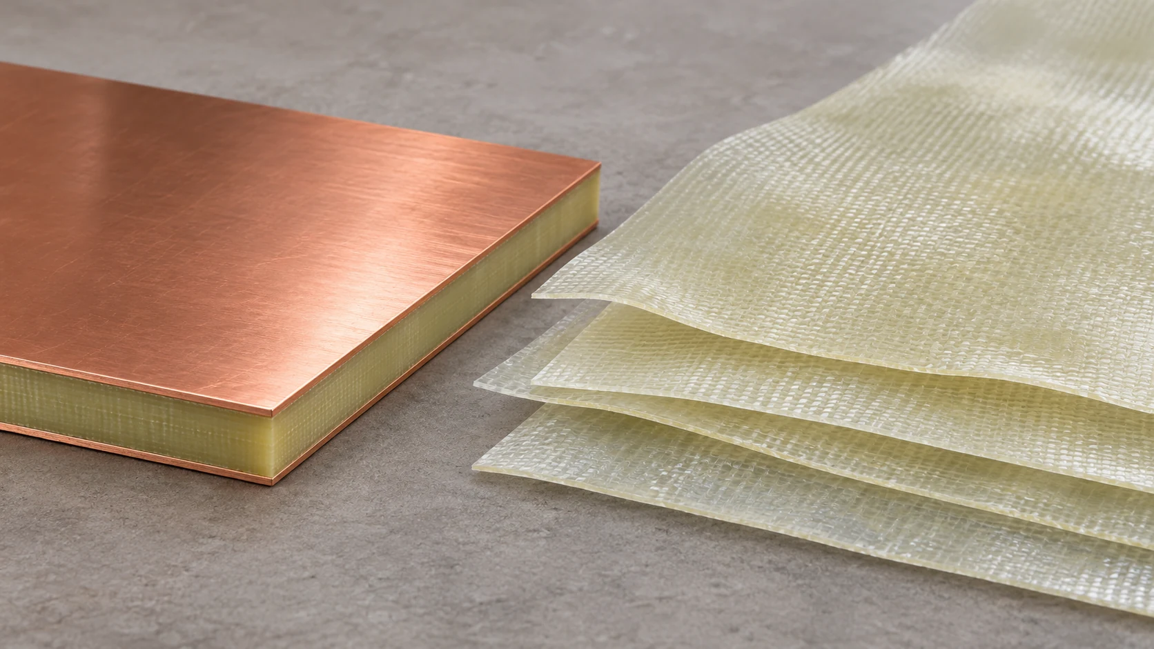
A PCB core is a consolidated, cured laminate, commonly supplied with copper on one or both faces. Prepreg is reinforcement impregnated with partially cured resin. During multilayer lamination, prepreg bonds adjoining materials, fills spaces around copper features and becomes part of the finished insulation system.
They are normally used together. The design decision is how to combine the cured laminate, bonding sheets and copper layers to achieve the required circuit geometry and buildable stackup. A label such as “FR-4 core” or “one sheet of 1080 prepreg” does not define the finished dielectric thickness or establish that the design will meet its impedance target.
A stackup identifies where each material form is used in the board. For a closer review of glass style, resin content and copper fill, see prepreg selection and resin content. For the raw copper-clad material itself, see copper-clad laminate.
Core and prepreg: the practical differences
| Question | PCB core | PCB prepreg |
|---|---|---|
| What arrives at the fabricator? | Consolidated laminate; often copper-clad | A sheet of reinforcement impregnated with partially cured resin |
| What does it contribute? | An existing dielectric region and, where clad, copper that can be patterned | Bonding and dielectric material between adjoining layers |
| What happens in multilayer pressing? | The laminate and its copper become part of the larger assembly | Resin flows and continues to cure during lamination |
| How should thickness be read? | Confirm the supplier's laminate definition, construction and tolerance | Confirm the proposed finished dielectric spacing after pressing, not only incoming sheet thickness |
| What should the drawing identify? | Material system, dielectric thickness, copper and any approved alternatives | Material system, required finished spacing, restrictions and permitted fabricator choices |
Core is not necessarily the geometric center or the thickest part of a board. A multilayer construction may contain several cores. Likewise, prepreg is more than an adhesive: once laminated, it also provides electrical insulation between conductors. The word “prepreg” on a finished stackup identifies how the region was formed; it does not mean the finished board contains loose, partially cured sheets.
These descriptions apply to common thermoset constructions. Material systems and bonding films differ; choose the combination and process using the applicable supplier documentation and fabricator's proposed build.
What is a PCB core?
A typical rigid PCB core consists of an insulating laminate with copper foil bonded to its surfaces. The fabricator images and etches copper where that core forms part of the intended layer structure. The cured laminate then separates the copper features on its faces.
A core can be useful when the design needs a defined copper-clad material construction from the laminate supplier. That does not mean every core with the same nominal thickness has the same electrical properties or that its dimensions have zero tolerance. Resin system, reinforcement, construction and copper foil can differ among products.
When the drawing specifies core thickness, resolve a simple but consequential question: does the stated thickness include only the dielectric, or the copper cladding as well? The order documentation should identify the convention, copper foil and acceptable tolerance. The finished board may also have different copper thickness on outer surfaces after plating, depending on the process and specified requirements.
A copper-clad core and a metal-core PCB are different uses of the word “core.” An insulated metal substrate includes a metal base and insulation system; it should not be assumed to follow the same construction as the glass-reinforced laminate discussed here.
What is PCB prepreg?
Prepreg is short for pre-impregnated reinforcement. In common rigid multilayer construction, it consists of glass reinforcement carrying a resin system in an intermediate cure state. The fabricator places the selected sheets between materials to be bonded, then applies a suitable lamination cycle.
As the construction is pressed, the bonding material must occupy spaces around neighboring copper patterns and form the finished insulating region. The amount and location of copper, chosen material, ply combination and process all affect the result. The incoming sheet thickness alone is therefore an incomplete description of the gap available for a signal layer after pressing.
A glass style is also only part of the specification. Sheets identified with the same style can be supplied with different resin contents or material systems. Confirm the complete material designation and the basis for any reported resin percentage. A larger percentage by itself is not a guarantee of void-free construction or a particular final thickness.
The material supplier's processing guidance applies to the specified products. It should not be presented as a universal lamination recipe for all prepregs or as proof of a specific board manufacturer's capability.
How do they fit into a four-layer PCB?
One common foil build starts with a double-sided copper-clad core for the two inner layers. The fabricator patterns the inner copper and laminates outer copper foil with prepreg on both sides. This is an illustration, not the only way to construct a four-layer PCB.
| Position in example | Supplied material or layer | Finished role |
|---|---|---|
| L1 | Outer copper foil, later processed | Top copper circuitry |
| L1–L2 | Selected prepreg construction | Bonded dielectric between outer and inner copper |
| L2 | Copper on one face of the core | Inner circuitry or reference plane |
| L2–L3 | Cured core laminate | Dielectric within the original core |
| L3 | Copper on the other face of the core | Inner circuitry or reference plane |
| L3–L4 | Selected prepreg construction | Bonded dielectric between inner and outer copper |
| L4 | Outer copper foil, later processed | Bottom copper circuitry |
The designer assigns electrical functions to L1 through L4. If a signal on L1 references a suitable continuous plane on L2, the L1–L2 dielectric and conductor geometry are central to that transmission structure. A design using a different reference arrangement must be analyzed with its actual field geometry and return path.
Other four-layer builds can use different core and bonding arrangements. Layer count alone does not settle which laminate forms, via sequences or processing steps will be used. Ask for the proposed construction before treating a generic layer diagram as an approved stackup.
Why nominal material thickness is not the same as a finished gap
For a core, first check whether the stated dimension includes copper. For prepreg, distinguish the incoming sheet from the finished dielectric in the actual build. The fabricator needs the copper geometry and material construction to propose a finished dielectric construction.
As a hypothetical stackup review, suppose a preliminary drawing identifies an L1–L2 finished dielectric target of 0.100 mm. The next proposal uses 0.080 mm for that same finished dielectric space. If every other thickness in the board were held constant, the board thickness subtotal would decrease by 0.020 mm. In a real board, other layers, conductor dimensions and tolerances may also change; the actual difference must be taken from the revised stackup.
The example is not a manufacturing tolerance, a prediction of the pressed result or an impedance calculation. Its purpose is to show that changing one dielectric can affect both the total thickness budget and the local geometry. A board can meet an overall thickness target while one critical signal-to-reference spacing differs from the model used for routing.
When comparing proposals, ask each supplier to identify:
- Finished overall board thickness and applicable tolerance.
- Material and finished dielectric spacing for each critical layer pair.
- Whether core dimensions include or exclude copper.
- Base and finished copper assumptions, including plating where applicable.
- Identified signal layers, reference layers and any critical structures.
Do not add a quoted incoming prepreg thickness to a core dimension and call the sum the final board thickness unless the supplier and fabricator have defined those numbers on that basis.
How do core and prepreg affect impedance and loss?
Both materials form part of the finished board's dielectric construction. Neither “core” nor “prepreg” alone determines impedance. A useful impedance model needs the intended conductor geometry, relevant dielectric construction, reference arrangement and appropriate material data.
For a controlled-impedance layer, ask the fabricator to state which spacing and copper dimensions were used in the model. Confirm whether trace widths are artwork values or finished requirements and how allowable manufacturing adjustments are handled. If a material is changed, agree whether the stackup and model must be reviewed again.
Dk and Df are not interchangeable. Dk is used in characterizing dielectric behavior relevant to propagation and impedance; Df describes dielectric loss under the reported test conditions. A complete insertion-loss assessment may also need copper roughness, conductor geometry, transitions and the rest of the signal channel. Avoid deciding that a board meets a channel budget solely because a laminate's data sheet lists a low Df.
The material data sheet reading guide explains the importance of test frequency and method. Where specified, an impedance coupon and report can support acceptance of agreed test structures; they do not automatically establish the performance of every net on the finished board.
Can a core be replaced with prepreg?
A finished dielectric region might be re-engineered using another combination of materials, but a one-for-one replacement should not be assumed. A core and a prepreg construction with the same nominal thickness can differ in supplied form, copper association, reinforcement, resin content, fabrication route and electrical properties.
Consider a proposed replacement as a stackup change, not as a wording change on the drawing. Ask:
- Which copper layer is supported or patterned on the existing core?
- How will the alternative be assembled and bonded?
- What finished spacing and copper geometry will be produced?
- Are the modeled Dk, Df and impedance assumptions still applicable?
- Does the change affect the manufacturing sequence, registration or via architecture?
- What new inspection or product qualification is required?
- Who must approve the change before fabrication?
The project owner defines functional and qualification requirements. The fabricator proposes a build and identifies its production constraints. A material supplier's data sheet supports the decision but does not, by itself, approve an untested board-level substitution.
What should an engineer provide with the stackup?
| Handoff item | Information that makes the review useful |
|---|---|
| Layer plan | Copper layer order, signal and reference functions, board outline and current revision |
| Material | Named family or approved alternatives, applicable restrictions and relevant supplier documentation |
| Dielectric | Overall thickness and critical finished dielectric targets, with the intended measurement basis and tolerances |
| Copper | Base or finished thickness by layer; artwork defining copper coverage and important local features |
| Electrical | Impedance targets, tolerances, associated structures and loss requirements where applicable |
| Construction | Via types and spans, relevant layer sequencing and any mechanical or thermal constraints |
| Verification | Requested test structures, methods, reports, acceptance criteria and treatment of changes |
Ask the fabricator to provide a proposed finished stackup showing the dielectric regions and assumptions used for impedance calculations. Review it together with the drawings and layer files before releasing the order. Availability, material substitution, tests and deliverables should be agreed for the individual project.
For broader context, the PCB materials guide compares substrate families, while multilayer PCB manufacturing covers the board category. Contact HILPCB or request a quote to discuss a specific build.
Frequently Asked Questions
Is prepreg the same as a PCB core?
No. A core is supplied as consolidated laminate, often with copper cladding. Conventional prepreg begins as reinforcement with partially cured resin and forms a bonding dielectric during lamination.
Does a four-layer PCB always have one core?
No. A foil build can use a central double-sided core and outer prepreg and foil. Other constructions are possible; the actual build depends on the design and fabricator.
Is prepreg thickness the finished dielectric thickness?
Not necessarily. The finished spacing depends on the construction, adjacent copper and lamination process. Use the fabricator's proposed finished value for the relevant space.
Can core and prepreg use the same resin family?
Compatible laminate and prepreg forms can belong to the same material system. Confirm the exact products and processing guidance instead of assuming that all materials with a similar family name are interchangeable.
Does using a core guarantee controlled impedance?
No. Impedance also depends on the signal and reference geometry, conductor dimensions, dielectric properties and manufacturing tolerances. Agree on the model and required verification.