An accurate PCB manufacturing quote is far more than a number—it's an engineering diagnosis of your design's feasibility, cost structure, and build path. Done right, a quote identifies risk early (before the first panel is cut), aligns materials and stackups with performance targets, and maps the fastest route from prototype to stable production. Whether you're building high-frequency RF modules, safety-critical automotive boards, or compact consumer products, this guide explains the core pricing drivers, the files we need, and the process HILPCB follows to deliver dependable quality at competitive pricing.
1. Why Accurate PCB Manufacturing Quotes Matter
When designs push limits—higher data rates, tighter density, mixed materials—manufacturing complexity scales quickly. A rigorous quote:
- Surfaces constraints early: copper balancing, drill-to-copper clearances, aspect-ratio limits, finish compatibility with assembly.
- Clarifies trade-offs: high-frequency laminates vs. enhanced FR4, backdrill vs. HDI microvias, ENIG vs. ENEPIG for wire bonding.
- Stabilizes timelines: realistic lead times based on materials, lamination cycles, and QA scope.
- Reduces total cost: panel optimization, standard core/prepreg choices, and reuse of tooling across SKUs.
For RF, automotive, and aerospace applications, this up-front diligence often prevents weeks of re-spins and unplanned expense.
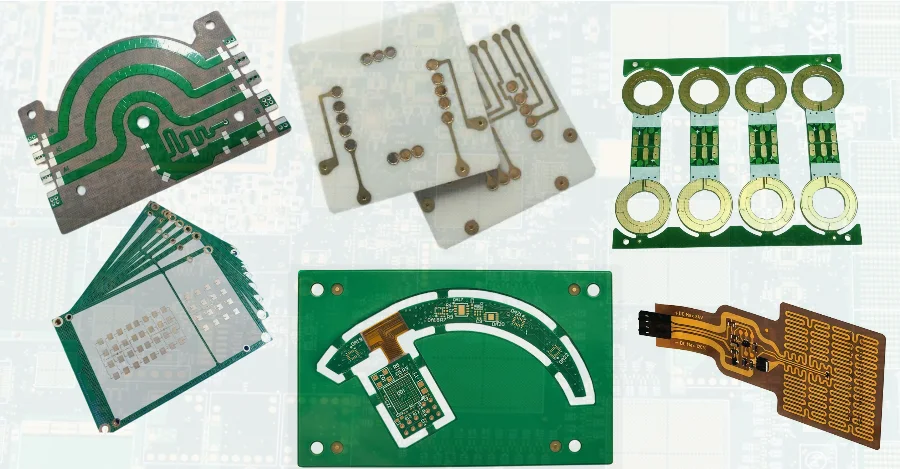
2. Key Applications for High-Quality PCB Manufacturing
We quote and build across diverse markets—each with distinct materials, tolerances, and compliance needs folded into the pricing model:
- Telecom & Networking: 5G base stations, 25G/56G+ SerDes backplanes, front-haul/back-haul RF cards
- Automotive Electronics: ADAS, EV BMS and on-board chargers, infotainment and telematics
- Industrial Control & Power: PLCs, robotics, drives, heavy-copper power distribution
- Medical Devices: imaging, diagnostics, patient monitoring with traceability and documentation
- Consumer & IoT: wearables, audio, smart home, with cost-sensitive, high-yield panelization
- Aerospace/Defense: rigid-flex navigation, high-reliability digital/RF hybrids
Each application affects material choice (Dk/Df, Tg), finish selection, acceptance criteria (IPC Class 2/3), and required test coverage—visible inside the quote.
3. Design Considerations for Manufacturing Success
Our engineering-first quoting process reviews your data package and proposes the most robust, cost-effective build. Key levers:
Stackup & Materials
- Standard FR4, high-Tg FR4, low-loss laminates (e.g., PTFE/Rogers-class), high-thermal substrates.
- Align impedances to standard dielectric thicknesses and copper weights to avoid exotic cores/prepregs.
Impedance Control
- Target ±5% with coupon placement; we document geometries and validate via TDR.
- Avoid unnecessary layer transitions; keep return paths tight to minimize skew.
Drill Strategy
- Manage aspect ratio (board thickness / finished via) for plating reliability.
- Choose between backdrill (remove stubs) vs. HDI microvias (0.10 mm laser) based on rate, density, and budget.
Copper Balancing & Warpage
- Symmetric stackups and uniform copper reduce bow/twist and lamination stress—critical for fine-pitch SMT.
Panelization
- CAD nesting to maximize ups per panel, consistent fiducials, and route-tab strategy that protects edge-plated features and castellations.
What to include with your RFQ (for fastest, most accurate pricing):
Gerber/ODB++, NC drill & route, fab drawing (dimensions, tolerances), proposed stackup, impedance table, copper weights, mask/legend, surface finish, specials (castellations, depth milling, peelable mask), acceptance class, and any required reports (COC/COA, microsection, TDR).
4. Manufacturing Challenges in Complex PCB Production
At HILPCB, we combine industry-leading maximum capabilities with high-yield, high-consistency production for mainstream complex PCBs. From 2-layer prototypes to 64-layer stackups and 20 oz extreme heavy copper boards, we have both the advanced equipment and process control to meet any challenge—whether your project demands cutting-edge complexity or consistent volume manufacturing.
Ultra High Layer Counts (Up to 64 Layers)
Producing very high-layer-count PCBs requires extreme registration accuracy and robust lamination control. Our advanced laser direct imaging (LDI), X-ray drill registration, and vacuum-assisted multi-opening lamination presses ensure perfect layer-to-layer alignment across sequential laminations. For boards over 30 layers, we use optimized resin systems and glass styles to mitigate CAF (Conductive Anodic Filament) risks and maintain dielectric thickness tolerances within ±5—10 μm.
HDI & Ultra-Fine Features
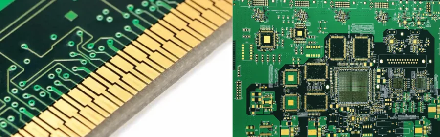
We support HDI designs up to any-layer interconnect, with 0.10 mm laser microvias, stacked or staggered configurations, and via-in-pad filled and capped for BGA pitches down to 0.20 mm. Fine-line imaging down to 75 μm trace/space is achieved using high-resolution LDI and optimized etch processes. This enables dense, high-speed designs for 5G, high-speed networking, and advanced computing without compromising yield.
Hybrid Stackups (RF + Digital + Embedded)
We specialize in mixed-dielectric builds that combine RF materials (Rogers, PTFE, Megtron, Taconic) with high-Tg FR4 for digital control sections. Sequential lamination, bond-ply optimization, and controlled-depth milling/laser cavity processing allow precise RF structures, embedded components, and thermal pockets without damaging neighboring layers—ideal for aerospace, defense, and high-frequency telecom.
Extreme & Heavy Copper (Up to 20 oz)
Our extreme heavy copper capability supports up to 20 oz (≈ 700 μm) copper thickness for power electronics, bus bars, and thermal management layers—while our mainstream heavy copper process (2—6 oz) is optimized for high yield in automotive, industrial, and LED applications. We design robust plating cycles, thermal relief features, and integrate metal-core PCB (MCPCB) solutions for optimal heat dissipation.
Surface Finishes & Assembly Readiness
We offer ENIG, ENEPIG, Immersion Silver, Immersion Tin, OSP, and Hard Gold finishes, each selected for fine-pitch assembly compatibility, wire bonding, or corrosion resistance. Our solder mask capability supports minimum dam widths of 75 μm and high-resolution LPI coating for ultra-fine pitch SMT. All boards are cleaned to ionic contamination standards for conformal coating and mission-critical assembly.
HILPCB's Strengths in Meeting These Challenges
- Breadth of Capability: From quick-turn 2-layer boards to 64-layer sequential lamination HDI and 20 oz extreme heavy copper
- Advanced Equipment: LDI exposure, UV & CO₂ laser drilling, X-ray drill alignment, automated via fill & planarization, precision CNC and laser routing
- Process Control: SPC monitoring at every critical step, AOI on every layer, μ-section analysis, impedance coupon validation
- Certifications & Standards: IPC Class 2/3, ISO 9001:2015, IATF 16949, UL, RoHS/REACH
- Engineering Expertise: Stackup co-design, impedance modeling, RF material selection, DFM optimization during quotation stage
By combining unmatched extreme manufacturing capabilities with robust, repeatable mainstream processes, HILPCB ensures that whether your requirement is a high-volume industrial board or a one-off 64-layer prototype, it will be delivered with precision, reliability, and industry-leading quality.
5. Performance Benefits of a Well-Manufactured PCB
- Signal Integrity: tightly controlled impedance, reduced reflections and via stubs, lower insertion/return loss.
- Mechanical Stability: low bow/twist, robust interconnects (through-hole, blind/buried, microvias).
- Reliability: material/finish choices matched to environment (thermal cycling, humidity, vibration).
- Compliance & Documentation: IPC Class 2/3 builds, ISO-aligned QMS, UL, RoHS/REACH, with traceable measurement reports.
A reliable board protects your design margins—and your brand.
6. Why Choose HILPCB for PCB Manufacturing
At HILPCB, every project starts with engineering at the core. We don't just send you a price—we deliver a technical roadmap for manufacturability, cost control, and performance optimization. Our quotations include full DFM analysis, stackup co-design, and built-in cost-reduction strategies such as material standardization, panel optimization, and reusable tooling. This engineering-first approach ensures your design is production-ready before the first panel is fabricated, saving both time and budget.
Our manufacturing capabilities span from mainstream production to industry-leading extremes. We can build 2—64 layer boards, complex HDI with stacked or staggered microvias, rigid-flex hybrids, and extreme heavy copper up to 20 oz for high-power applications. Fine-line imaging down to 75 μm trace/space, controlled-depth routing, and precise backdrill capability allow us to meet the demands of high-frequency, high-speed, and automotive-grade electronics with consistent, repeatable quality.
We deliver speed without sacrificing precision. Standard prototypes can ship in 24—72 hours, while complex multilayers are typically ready in 5—7 working days. Every board undergoes 100% electrical test, AOI on every layer, and X-ray inspection for hidden features. Impedance-controlled builds are verified to ±5% with TDR, and all products meet IPC Class 2/3, ISO 9001:2015, IATF 16949, UL, and RoHS/REACH standards. With HILPCB, you gain a partner who combines engineering expertise, extreme manufacturing capability, and uncompromising quality to ensure your project's success.
7. Frequently Asked Questions (FAQ)
Q1: How is price formed in a PCB manufacturing quote?
A: Core drivers are stackup complexity, material system (and sourcing risk), feature density (min trace/space, via types), finish, panel utilization, and QA scope. We also factor NRE/tooling and, for HDI, sequential lamination counts.
Q2: What can I do to lower cost without hurting performance?
A: Align impedances to standard dielectric thicknesses, consolidate via sizes, avoid exotic mask colors/finishes unless required, balance copper, and allow panel-friendly outlines. We'll propose options in the quote.
Q3: How fast is quoting and prototyping?
A: Standard designs quote within hours; complex HDI/RF in 4—6 hours after engineering review. Prototypes ship in 24—72 hours for common builds; complex multilayers typically 5—7 days.
Q4: Do you guarantee impedance control?
A: Yes. We design and place coupons, validate with TDR, and target ±5% tolerance, with documented results attached to the lot.
Q5: Can you support automotive/industrial reliability?
A: We build to IPC Class 3 where required, support IATF-aligned controls, and offer extended QA (thermal cycling, humidity, salt fog) with full traceability.
Q6: Do you also handle assembly and supply chain?
A: Yes—our turnkey service integrates fabrication with SMT/THT assembly, test, and authorized component sourcing, reducing total lead time and cost.