

HILPCB provides PCB manufacturing and assembly support, including rework planning for incorrect placements, solder defects and engineering changes. Each proposed correction requires an assessment of component condition, laminate limits, schedule and inspection requirements; turnaround depends on the scope and available equipment.
An integrated fabrication and assembly workflow can reduce supplier handoffs and provide useful board-construction data during rework. Turnaround and pricing depend on defect severity, component availability and agreed project terms.
Professional rework maintains board integrity and product reliability. Amateur techniques lift pads, damage traces, and create hidden failures. Rework should follow documented, package-specific procedures and use the acceptance criteria agreed with the customer; personnel credentials should be checked for the relevant current certification.
Why Integrated Manufacturing + Assembly + Rework Matters
Split-vendor problems:
- Communication delays coordinating multiple suppliers
- Unclear responsibility when issues arise
- Extended lead times shipping boards for external rework
- Additional costs for shipping and rework services
HILPCB integrated advantage:
Our facility handles PCB manufacturing (2-64 layers), SMT/through-hole assembly, and professional rework under one roof:
- Faster response: Issues corrected immediately, same facility
- Better results: Rework technicians know board construction details from our PCB engineering process
- Clear accountability: Single point of contact for entire project
- Cost efficiency: Fewer supplier transfers; rework charges depend on contract terms
BGA Rework: Critical Capability
Modern electronics rely on expensive BGA packages ($5-$50+) mounted on valuable boards ($50-$500). When X-ray inspection reveals voids or components fail, professional BGA rework becomes essential.
Because we manufacture the PCB, HILPCB’s IPC-trained technicians perform professional rework in-house and understand how thermal characteristics, copper weights and laminate properties affect repair. Split-vision placement can achieve ±0.05 mm on qualified package and pad designs; actual accuracy depends on station calibration and geometry. Same-day correction may be available for eligible jobs. Training and qualification are personnel-specific and do not imply a current corporate IPC certificate; each repair follows its package profile and approved acceptance criteria.
Equipment and process:
- Vision-assisted component alignment; achievable accuracy depends on station calibration, package and pad design
- Temperature profiling with multiple thermocouples
- Board preheating to a measured, package-specific profile to control thermal gradients
- Controlled removal following component reflow profile
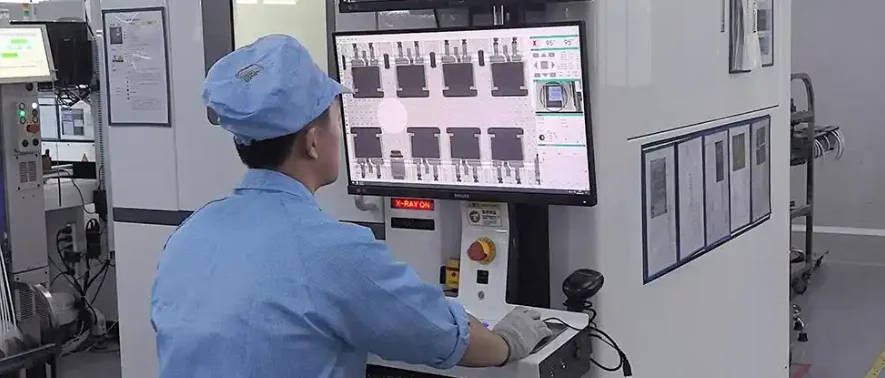
- X-ray inspection using acceptance criteria specified for the BGA package and application; do not apply QFN thermal-pad void limits to BGA solder balls
Removal procedure:
- Preheat the board according to the validated component and board profile
- Apply localized heat following reflow profile
- Remove package when slight movement indicates full reflow
- Clean the pads while the solder remains molten, following the approved rework procedure
- Inspect under magnification for damage
Common failures prevented:
- Pad lifting: Precise temperature control, avoid exceeding limits
- Board warpage: Preheat entire board, not just local area
- Adjacent damage: Shield nearby components with heat-resistant materials
Replacement validation:
- Vision-assisted placement verified against package- and station-specific alignment limits
- Package-specific reflow profile
- X-ray inspection verifying joint quality through comprehensive PCB inspection
- Electrical testing before completion
HILPCB’s documented historical BGA first-pass result exceeded 98% within its recorded scope; report current yield against the component mix, sample size and observation period. See our PCB repair services for further process considerations.
SMT Component Rework
Surface mount components from tiny 0201 resistors through large QFP processors require different rework approaches.
Small passives (0201-1206):
- Hot air or hot tweezers removal
- Use a controlled, measured heating profile compatible with the solder alloy and component limits
- Heat both pads simultaneously preventing tombstoning
- Inspect under magnification verifying fillet formation
IC packages (SOIC, QFP, QFN):
- Appropriately-sized hot air nozzle
- Temperature profile brings all pins to reflow simultaneously
- Remove when package shifts slightly
- Inspect for bridges, insufficient solder, or pad damage
- Replace with proper pin alignment and even heating
Illustrative rework profile checkpoints (not universal temperature specifications):
- Preheat: set ramp and board temperature using thermocouples and the approved rework profile
- Soak: allow the package and board to equilibrate without exceeding component exposure limits
- Reflow: confirm the solder alloy reaches liquidus while respecting package peak-temperature and time-above-liquidus limits
- Cooling: follow a controlled cooldown compatible with laminate and component requirements
ECO Implementation
Engineering Change Orders during product development benefit from our integrated facility. Design changes get implemented efficiently without external coordination, supporting rapid PCB development cycles.
Common ECO types:
Component value changes: Simple resistor/capacitor value substitutions completed quickly. Verify correct values preventing errors.
Component type changes: When footprints differ:
- Jumper wires bridging pad spacing differences
- Unused pad removal preventing shorts
- Mechanical fitment verification
Trace modifications:
- Scrape solder mask, cut trace completely
- Verify cut with continuity tester
- Route jumper wires with appropriate gauge
- Apply solder mask repair preventing shorts
- Secure wires with UV adhesive
Firmware updates: Hardware modifications coordinated with programming updates ensuring complete verification through PCB testing.
Quality Standards and Inspection
For rework, use IPC-7711/7721 as the relevant procedure guidance where contracted, J-STD-001 for applicable soldering requirements and IPC-A-610 for finished-assembly acceptability. Visual inspection must use the criteria and coverage agreed for the assembly class and defect type:
- Solder joint quality (fillet formation, wetting, volume)
- No bridges or shorts to adjacent conductors
- Component placement and orientation correct
- Mechanical stability without looseness
- Cleanliness without excessive flux residue
Electrical verification:
- Continuity testing verifies intended connections
- Isolation testing confirms no unintended shorts
- Functional testing validates circuit operation
- In-circuit testing when available
Documentation: Complete traceability including issue description, components affected, procedures performed, inspection results, test data, technician identification, and photographs. Critical for regulated industries requiring detailed quality records.
Rework vs Rebuild Decision
Our integrated facility enables honest evaluation. Sometimes rework makes sense; sometimes rebuilding proves more economical through PCB replication or PCB copying services.
Rework makes sense:
- Limited quantity affected
- Board value exceeds rework cost significantly
- Schedule critical, replacement lead time unacceptable
- Prototype/validation units where cosmetics less important
Rebuild makes sense:
- Extensive damage requiring multiple repairs
- High-volume production where rework creates bottleneck
- Rework cost approaches replacement cost
Decision points:
Prototypes (5-50 boards):
- Example rework cost: request a component-, batch- and labor-specific estimate
- Example replacement cost: include fabrication, component procurement and testing
- Decision: Compare total expected cost, process risk and production schedule
Production (100+ boards):
- Example rework cost: evaluate labor, reinspection and yield risk
- Example replacement cost: evaluate panel economics, component costs and lead time
- Decision: Compare the expected cost per accepted board; there is no universal defect-rate cutoff
Our project managers provide honest recommendations based on technical feasibility, cost, and schedule impact.
Integrated Factory Advantage
Investment in complete rework capability supports quality commitment:
Equipment:
- BGA rework stations ($20,000-$50,000)
- X-ray inspection ($80,000-$150,000)
- Vision systems ($15,000-$30,000)
- Temperature profiling equipment
- Specialized tooling and fixtures
Technician expertise:
- Training and, where applicable, verified IPC-A-610, J-STD-001 and IPC-7711/7721 credentials
- Experience across component types and technologies
- Thermal management understanding
- Continuous education with package evolution
Advantages throughout project:
During manufacturing: Quality control catches issues early, immediate correction before assembly
During assembly: Multiple inspections (SPI, AOI, X-ray) identify issues, in-house correction maintains production flow
During testing: Immediate diagnosis and correction accelerates debug cycles, especially valuable for prototypes
For ECOs: Design changes implemented efficiently with internal coordination
Customer example: Illustrative workflow (not a verified customer case): A prototype batch with BGA voiding may be assessed by X-ray, reworked using a controlled thermal profile, and reinspected and electrically tested. Actual cost and lead time depend on defect extent, component stock and customer acceptance criteria.
Complete PCBA Services
PCB Manufacturing:
- 2-64 layer boards, FR-4 to Rogers materials
- Advanced capabilities: blind/buried vias, impedance control
- Full electrical testing
Assembly:
- SMT: 01005 components through fine-pitch BGAs
- Through-hole: wave and selective soldering
- Prototype to production volumes
Quality assurance:
- Solder paste inspection, first article inspection
- AOI, X-ray inspection
- Functional testing per requirements
- Professional rework capability included
Engineering support:
- DFM review, component selection
- Test development, ECO planning
- Failure analysis through PCB reverse engineering
- Corrective action and PCB cloning for legacy support
Conclusion
HILPCB delivers complete PCBA solutions from bare board fabrication through final assembly with professional rework capability:
- Single-source accountability for quality
- Faster turnaround without external coordination
- Professional rework with IPC-certified technicians
- Cost transparency with fair pricing
- Quality commitment backed by in-house capability
Visit HILPCB to discuss PCB manufacturing and assembly requirements.
Frequently Asked Questions
How do you desolder a component from a PCB?
First identify whether the joint is through-hole or surface-mount and check the component and board thermal limits. Apply suitable flux; use solder wick or a desoldering tool for through-hole joints, and controlled hot air or a rework station for suitable SMD packages. Avoid pulling components before the joints are fully molten.
Can you safely desolder a battery pack from a PCB?
Battery-pack rework carries short-circuit, thermal-runaway and fire risks. Disconnect and isolate the energy source using manufacturer-approved service procedures. Do not apply direct heat to cells or cut live interconnects; refer pack repairs to qualified personnel when the design is not explicitly serviceable.
What can replace solder wick for removing solder?
A temperature-controlled desoldering pump or vacuum station may remove molten solder from suitable joints. Use appropriate flux and follow a validated rework procedure. Do not flick or shake molten solder from a PCB because it can create shorts, burns and contamination.
What is PCB assembly rework, and how does it differ from repair?
Rework restores an assembly to applicable drawings or acceptance criteria; repair restores functionality or usability through an authorized deviation from the original design. IPC-7711/7721 includes both rework and repair guidance; the distinction is not simply factory work versus field work.